Last Updated
November 20, 2011
|
HOMEPAGE OF DR MANOJ SAXENA |
|
|
Dr. Manoj Saxena Senior Member-IEEE(USA), MIET(UK),
MInstP(UK), Life Member-NASI(Allahabad,India), Associate-IASc(Bangalore,
India) Assistant Professor, Department of Electronics Deen Dayal Upadhyaya College, University of Delhi, Karampura,
New Delhi-110015, India E : mail : saxenamanoj77@gmail.com, msaxena@ieee.org Tel: 91-011-25458173, Fax:
91-011-25173400 |
|
|
Membership
of Professional Societies Teaching Experience and Courses Taught
Research Guidance/ Supervision
Workshop/ Conferences Organized |
Brief CV
Dr. Saxena has reviewed extensively
for IEEE TRANSACTIONS
ON ELECTRON DEVICES, Semiconductor Science Technology,
Solid State Electronics, Journal of Physics: D Applied Physics, Superlattices
and Microstructures, Elsevier Science, UK, International Journal of Numerical
Modeling: Electronic Networks, Devices and Fields, Wiley, Journal of Electrical
and Electronics Engineering Research (JEEER), MAPAN-Journal of Metrology
Society of India and International Journal of Science and Technology
Education Research.
His name appeared in the Golden List of IEEE
Transactions on Electron Devices Reviewers since 2005.� He is also listed in the 25th
Anniversary edition of Who�s Who in the World. He is Member of National
Academy of Sciences India (NASI), Allahabad, India,� Institution of Engineering and Technology
(IET), UK, and International Association of Engineers, Hong Kong, Life Member of Semiconductor Society of India, New
Delhi, India, Life Member of Indian Science Congress
Association (ISCA), Young Associate of Indian Academy of Sciences (IAS), Bangalore, India and Joint
Secretary of Society for VLSI and
Microelectronics, New Delhi, India and Secretary of IEEE EDS Delhi Chapter, New Delhi He was Secretary of
Mini-Colloquia on Compact Modeling of advance MOSFET structures and mixed
mode applications on January 5-6, 2008 and The 18th WIMNACT(Workshop and IEEE
EDS Mini-colloquium on NAnometer CMOS Technology)-New Delhi, India -
Mini-Colloquia on Compact Modeling and Fabrication techniques of advance
MOSFET/ HEMT structures, June 04-05, 2009 at University of Delhi South
Campus, New Delhi, India sponsored by the IEEE Electron Device Society under
its Distinguished Lecturer Program. He was also Symposium Secretary of
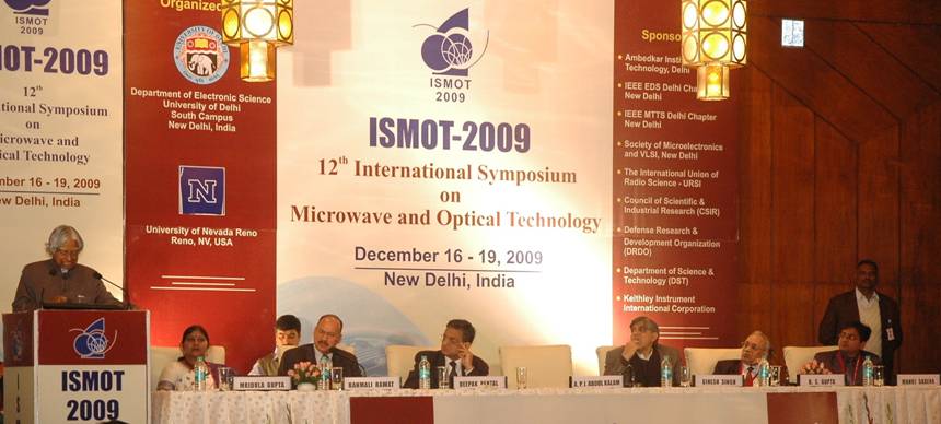
International Symposium on Microwave and Optical Technology (ISMOT)-2009 ,
December 16-19,2009 in Hotel Ashok, New Delhi, India He was Program Committee Member of Several
International Conferences and Workshops including India-Japan Workshop (IJW-2006) on
ZnO Materials and Devices, December 18-20, 2006 sponsored by DST (New Delhi)
- JSPS (Japan) organized by Department of Electronic Science, University of
Delhi South Campus, The Seventh International Conference on Distributed
Computing and Internet Technology, Bhubaneswar, India, 9- 12 February 2011,
International Conference on Soft Computing for Problem Solving (SoCProS
2011), Roorkee, India, December 16-18, 2011, MOS Modeling and Parameter
Extraction Working Group - MOS-AK/GSA Workshop, March 14-15, 2012. |
Academic
Background
- B. Sc (Honours) Electronics,
- M. Sc Electronics,
- Ph. D Electronic Science,
(Doctoral
Thesis - Physics based analytical modeling and simulation of Dual Material
ate (DMG) MOSFET)
Work Experience
- Lecturer, Department of Electronics, Deen Dayal Upadhyaya College, University of Delhi (August 2000 - December
2005)
- Assistant Professor, Department of Electronics, Deen Dayal Upadhyaya College, University of Delhi (01/01/2006 � 30/08/2006)
- Assistant Professor (Lecturer in Senior Scale),
Department of Electronics, Deen
Dayal Upadhyaya College, University of
Delhi (30/08/2006 � 30/09/2009)
- Assistant Professor (Reader), Department of
Electronics, Deen Dayal Upadhyaya
College, University of Delhi (30/08/2009
- Till Date)
Award and Honors
- Received Smt. Shanti Devi
Bhargava Memorial Gold medal for being best candidate in the M. Sc
Examination in Electronics in 2000
- Name appeared in
the Golden List of IEEE Transactions on Electron Devices
Reviewers for year 2005, 2006, 2008, 2009 and 2010.
Special Achievements: -
- Name listed in the 25th Anniversary edition of Who�s Who in the World.
- Research
work has been highlighted in The Telegraph newspaper, April
14, 2003
- Reviewer of IEEE Transactions on
Electron Devices
- Reviewer of Journal
of Physics D: Applied Physics, Institute of Physics (IOP))
- Reviewer of Semiconductor
Science Technology, Institute of Physics (IOP))
- Reviewer of Solid
State Electronics, Elsevier Science, UK �
- Reviewer of Superlattices
and Microstructures, Elsevier Science, UK
- Reviewer of International
Journal of Numerical Modeling: Electronic Networks, Devices and Fields,
Wiley
- Reviewer of IET
Micro and Nano Letters
- Reviewer of Journal
of Electrical and Electronics Engineering Research (JEEER)
- Reviewer of MAPAN-Journal
of Metrology Society of India
- Reviewer of International
Journal of Science and Technology Education Research
- Reviewer of International
Conference - Asia Pacific Microwave
Conference (APMC)-2008, 16-19, December 2008 in Hong
Kong Convention and Exhibition Center, Hong Kong, China
- Reviewer of International Conference - International
Symposium on Microwave and Optical Technology (ISMOT)-2009,16-19, December 2009 in Hotel Ashok, New Delhi, India
- Reviewer for Book Proposal for Universities Press
(India) Pvt. Ltd. Hyderabad. (2009 - )
- Reviewer for The 8th International Conference
on Computing, Communications and Control Technologies: CCCT 2010, Jointly
with The 16th
International Conference on Information Systems Analysis and Synthesis:
ISAS 2010, In the Context of The
International Multi-Conference on Complexity, Informatics and Cybernetics:
IMCIC 2010, April 6th - 9th,
2010 Orlando, Florida USA
- Reviewer of� National Conference on
Recent Trends in Exotic materials (NCRTEM 10), Sharda University Greater
Noida-201306, U.P., India
- Reviewer for 7th International Conference on Distributed
Computing and Internet Technologies (ICDCIT � 2011), Bhubaneswar during 9
� 12 February 2011.
- Member-Review
Committee - International Conference on Latest Trends in Nanoscience
and Nanotechnology (ICNSNT), 28th -29th� March 2011, Karnataka, India
- Reviewer of The SPRING 9th International Conference on Computing,
Communications and Control Technologies: CCCT 2011� Jointly with The 17th International
Conference on Information Systems Analysis and Synthesis: ISAS 2011 In the
Context of The 2nd International Multi-Conference on Complexity,
Informatics and Cybernetics: IMCIC 2011, March 27th - 30th, 2011 ~
Orlando, Florida USA
- Reviewer for
The 4th International Multi-Conference on Engineering and Technological
Innovation: IMETI 2011, July 19th - July 22nd, 2011 � Orlando, Florida,
USA
- Reviewer of International Symposium on Models and Modeling
Methodologies in Science and Engineering: MMMse 2011� in the context of The 15th World
Multi-Conference on Systemics, Cybernetics and Informatics: WMSCI 2011, July
19th - July 22nd, 2011 � Orlando, Florida, USA
Membership of Professional
Societies/ National Level Committees
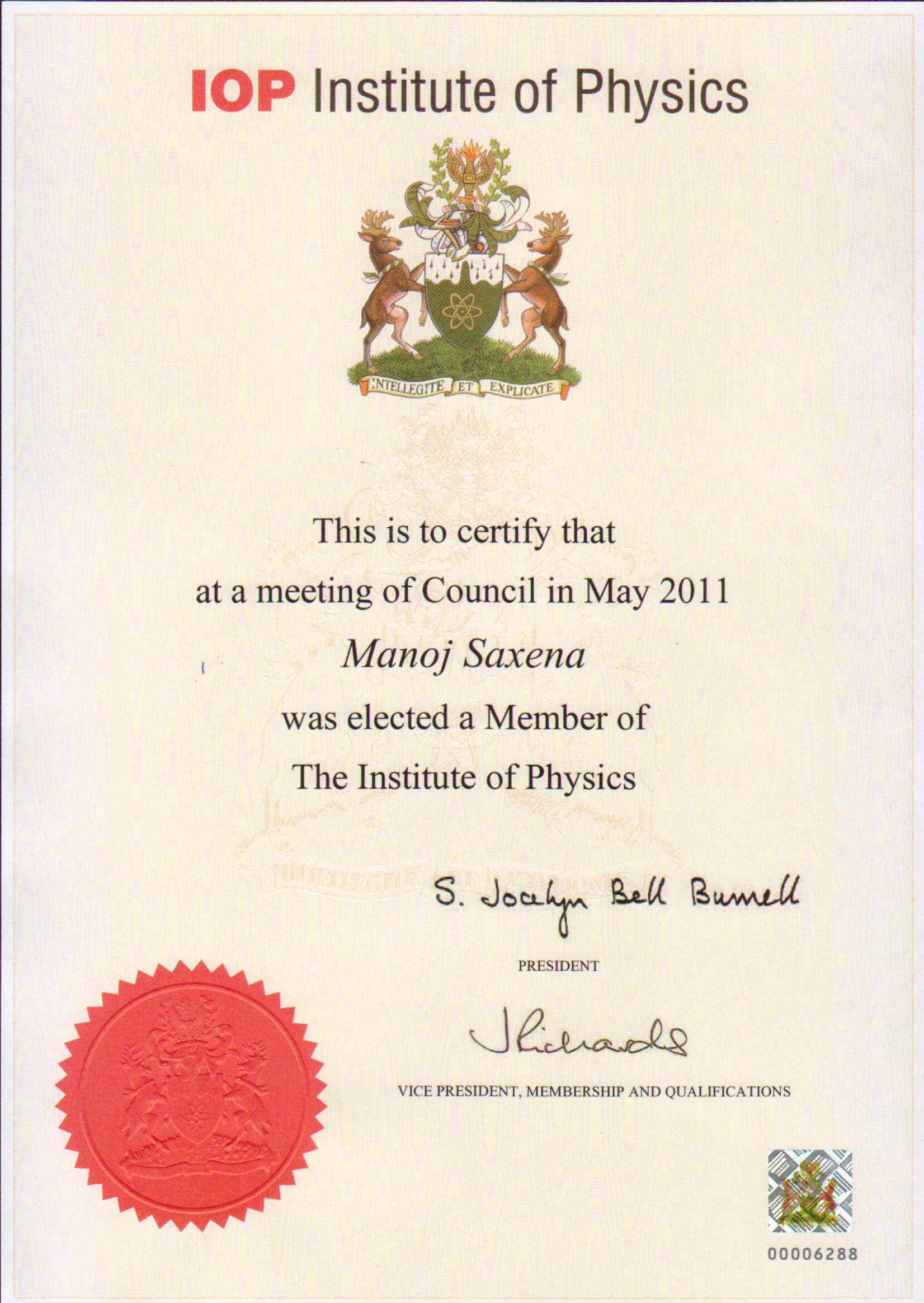
- MInstP - Member �
Institute of Physics (IOP), UK in May 2011 (at
the Age of 33)
- Expert Member �- Directory of researchers working in the
country in the area of Nano Science and Technology, Nano Mission, Department of Science and Technology,
Govt. of India (at the Age of 32)
- Associate
� Indian Academy of Sciences (IAS), India (2009 - (at the Age of
32)
- M. N. A. Sc � Member, National Academy of Sciences
India (NASI), Allahabad, India (2009 - ) (at the Age of 31)
- Senior Member � IEEE, USA (July 2008) (at the Age of 30)
- MIET - Member
� Institution of Engineering and Technology (IET), United Kingdom (UK) (2008-)
- Secretary �
IEEE EDS Delhi Chapter, New Delhi, India (2010 � Till date)
- Member - International
Association of Engineers, Hong Kong (Membership
No: 64986)
- Life Member � Semiconductor Society of India,
New Delhi,
- Life Member - Indian Science
Congress Association (ISCA) (Membership No. L13169)
- Joint Secretary � Society for VLSI and
Microelectronics, New Delhi, India (2008-)
- Joint
Secretary and Treasurer � IEEE EDS Delhi Chapter, New Delhi, India (2009)
- Member � Electronic Devices Society, USA (2008-)
Sponsored Projects:-
- Co-Principal Investigator in UGC, Govt. of India sponsored research project entitled Modeling
and simulation of Nanoscale Dual Material Gate Insulated Shallow Extension
Silicon on Nothing MOSFET for Low voltage low power applications (F.
No. 36-258/2008(SR)) worth Rs. 9,22,800
On Going - (May 2009 � Till Date)
- Co-Project
Investigator in
a DRDO sponsored Project entitled Physics Based Modeling and
Simulation of Sub-100 nm recessed channel (RC) and insulated shallow
extension (ISE) MOSFET with gate electrode work function engineering
structures for high performance applications (ERIP/ER/0803693/M/01/1258)
worth Rs. 4.70 lakhs
On Going - (October 2010 � Till Date)
�
Co-Project Investigator in a DRDO sponsored Project entitled Physics Based
Modeling Simulation and Electrical Characterization of a Novel Device
Architecture: Silicon-On-Nothing MOSFET for Sub-100 nm Device Dimensions (No. ERIP/ER/0303417/M/01) worth Rs.
31.68 Lakhs
Completed - (April-2004-December
2007)
Book Chapters: -
- Member - Editorial Board - Proceedings
of 16th Asia Pacific Microwave Conference 2004, Department of Electronic
Science, University of Delhi, Allied Publishers Pvt. Ltd. 2004, ISBN
81-7764-722-9.
- Book Chapter - MOSFET
Modeling, R. S. Gupta, Mridula Gupta and Manoj Saxena, Encyclopedia
of RF and Microwave Engineering, John-Wiley & Sons, Inc. New Jersey,
USA, March 2005, pp. 3278-3317, ISBN: 0-471-27053-9.
- Proceeding Editor - National
Conference on Mathematical Techniques: Emerging Paradigms for Electronics
and IT Industries (MATEIT-2006) from 22nd March � 25th
March 2006, Deen Dayal Upadhyaya College, University of Delhi, Shivaji
Marg, New Delhi, India, ISBN: 81-8424-026-0
- E-Proceeding Editor - National
Conference on Mathematical Techniques: Emerging Paradigms for Electronics and
IT Industries (MATEIT-2008) from 26th September � 28th
September 2008, Deen Dayal Upadhyaya College, University of Delhi, Shivaji
Marg, New Delhi, India
- Editor �
Proceeding of the International Symposium on Microwave and Optical
Technology (ISMOT)-2009, December 16-19, 2009.
- Proceeding Editor - Third
National Conference on Mathematical Techniques: Emerging Paradigms for
Electronics and IT Industries (MATEIT-2010) held during January 30-31,
2010, Deen Dayal Upadhyaya College, University of Delhi, Shivaji Marg, New
Delhi, India, sponsored By University Grants Commission (UGC), Govt. of
India
�
Teaching
Experience and Courses Taught
Post Graduate Level (As Visiting Faculty)
|
Course |
Year |
|
M. Sc Electronics (IVth
Semester) - VLSI Circuit Design and Device
Modeling � 4.2 (Deptt.
Of Electronic Science, University of Delhi South Campus) |
Jan 2011 � April 2011 |
|
M. Sc Electronics (Ist
Semester) - Advance Analog and Digital Electronics - 1.4 (Deptt.
Of Electronic Science, University of Delhi South Campus) |
July 2011 � December 2011 July 2010 � December 2010 July 2009 � December 2009 July 2008 � December 2008 July 2005 � December 2005 July 2004 � December 2004 |
|
M. Sc Informatics � Introduction to
Communication Systems � IT-13 (Institute of
Informatics & Communication, University of Delhi South Campus) |
2005-2006 |
Under Graduate Level
|
Course |
Year |
|
B. Sc. (H) Electronics III Semester � Analog Electronics-I |
July 2011-November 2011 |
|
B. Sc. (H) Electronics II
Semester � Signal and Systems |
January 2012-April 2012 January 2011-April 2011 |
|
B. Sc. (H) Electronics I Semester � Network Analysis |
July 2010-November 2010 |
|
B. Sc. (H) Electronics I year � Network Analysis and Linear
Active circuits |
2008-2009 2007-2008 2004-2005 2003-2004 2002-2003 |
|
B. Sc. (H) Electronics II year � Operational Amplifier and
Analog Computation |
2009-2010 2008-2009 2007-2008 2006-2007 2005-2006 |
|
B. Sc. (H) Electronics II year � Numerical analysis and FORTRAN
programming |
2008-2009 2007-2008 |
|
B. Sc. (H) Electronics III year � Engineering Drawing |
2003-2004 |
|
B. Sc. (H) Electronics III year � Power Electronics |
2006-2007 2005-2006 |
|
B. Sc. (H) Electronics III year � Communication System |
2003-2004 2002-2003 |
|
B. Sc (H) Computer Science I semester� - Digital Electronics |
2006-2007 2005-2006 2004-2005 |
|
B. Sc (H) Computer Science II semester� - Analog Electronics |
2003-2004 |
|
B. Sc (H) Computer Science V semester� - Microprocessor |
2004-2005 2003-2004 |
�
External
Examiner
�
External Examiner of M. Tech thesis � School of
Computer Science, Jawaharlal Nehru University, New Delhi, India from 2008
onwards.
Research Guidance/ Supervision
Joint Supervision
|
S. No. |
Title |
Candidate�s
name and Affiliation |
Year |
Status |
|
|
Modeling and
simulation of Nanoscale Dual Material Gate Insulated Shallow Extension
Silicon on Nothing MOSFET for Low voltage low power applications |
Ms. Vandana Kumari, Research Scholar,
UGC-NET (LS) Department of Electronic Science, University of Delhi South Campus, New
Delhi. |
Jan-2010 |
On Going |
Mentor for the Research Scholar
|
S. No. |
Title |
Candidate�s
name and Affiliation |
Year |
Status |
|
|
Analytical
Modeling and Simulation of Tunnel FET |
Ms. Rakhi Narang, Research Scholar,
UGC-JRF-NET, Department of Electronic Science, University of Delhi South Campus, New
Delhi. |
Jan-2010 |
On Going |
|
|
Analytical
Modeling and Simulation of Optically Controlled FET (OPFET) |
Ms. Rajni Gautam, Research Scholar,
UGC-JRF-NET, Department of Electronic Science, University of Delhi South Campus, New
Delhi. |
Jan-2010 |
On Going |
At
National Level
(Summer
Research Fellowship Sponsored by Indian Academy of Sciences (IAS), National
Academy of Sciences, India (NASI) & Indian National Science Academy (INSA))
|
S. No. |
Title |
Candidate�s name
and Affiliation |
Duration |
Status of
Project |
|
|
Computer Aided Analysis,
Charecterization, Optimization and Simulation of Bio-Molecules of Field
Effect Biosensors |
Jagriti Mishra B. Tech, BITS Meshra (ENGS1368) |
May-July2010 |
Completed |
|
|
Analytical
modeling and Simulation of Short Channel Effects and Quantum-Confinement
Effects in Silicon Nanowire MOSFET |
Gaurav Mahajan B.E. (Hons.) Electrical and Electronics Engineering Birla Institute of Technology and Science, Pilani (ENGS2982) Publication 1. A 2-D Subthreshold Analytical model
for Short Channel Effects in Nanowire MOSFETs (Si, Ge), Gaurav Mahajan, Rakhi
Narang, Manoj
Saxena, V.K. Chaubey, Nirma University International Conference on
Engineering (NUiCONE) 2010, December
09-11, 2010, Nirma University, Ahmedabad 2. Mixedmode Circuit Simulation of
Silicon and Germanium Nanowire MOSFETs - A Comparative Study,Gaurav Mahahan,
Rakhi Narangi, Manoj Saxena and V.
K. Chaubey, 2011 IEEE Students'
Technology Symposium, IIT Kharagpur during 14-16 January 2011. |
May-July2010 |
Completed Currently
studying MS in Electrical Engineering at Stanford University, USA |
|
|
Analytical
modeling and Simulation of Germanium on Insulator MOSFET for Optical
Application |
Neha Bhushan KIIT University, Bhubaneswar (ENGS2269) |
May-July2011 |
Completed |
|
|
Analytical
modeling and simulation of Tunnel FET for Sensor application |
K V Sasidhar Reddy NIT, Warangal (ENGS4147) Publication 1.
Analytical
Model of a Tunnel FET Based Biosensor for Label Free Detection, Rakhi
Narang, K V
Sasidhar Reddy, Manoj Saxena, R. S. Gupta and Mridula Gupta, Accepted for
Publication in 2011 International Semiconductor Device Research Symposium,
December 07-09, 2011, University of Maryland, USA |
May-July2011 |
Completed |
At
College Level
Under Graduate Students (As Guide):����������� 09
|
S. No. |
Title |
Candidate�s name and Affiliation |
Year |
Status |
|
|
Implementation of a Nanoelectronic Full Adder and
Nano-circuit to control millimeter scale walking robot |
Sumit Jain B. Sc. (H) Computer Science- Sixth Semester Deen Dayal |
2007 |
Completed |
|
|
HeRMES:
High-Performance Reliable MRAM-Enabled Storage and On-chip MRAM as a
High-Bandwidth, Low-Latency Replacement for DRAM Physical Memories |
Angad Singh B. Sc. (H) Computer Science- Sixth Semester Deen Dayal |
2007 |
Completed |
|
|
Banked
Microarchitectures for Complexity-Effective Superscalar Microprocessors |
Gaurav Arora B. Sc. (H) Computer Science- Sixth Semester Deen Dayal |
2007 |
Completed |
|
|
Handwriting Recognition Using Artificial Neural Networks |
Sagar Rangra B. Sc. (H) Computer Science- Sixth Semester Deen Dayal |
2008 |
Project Engineer Wipro
Technologies, Electronic City, Bangalore � 560100 |
|
|
Data And Picture Encryption Using
Image Processing |
Ankit Bhatia B. Sc. (H) Computer Science- Sixth Semester Deen Dayal |
2008 |
Completed |
|
|
Pattern Recognition |
Preeti Duhan B. Sc. (H) Computer Science- Sixth Semester Deen Dayal |
2008 |
Completed |
|
|
Expert System
Architecture |
Garima Arora B. Sc. (H) Computer Science- Sixth Semester Deen Dayal |
2008 |
Currently Instructional
Designer NIIT
Technologies Limited, Kalkaji |
|
|
Neural Networks |
Saarthak
Shandilya B. Sc. (H) Computer Science- Sixth Semester Deen Dayal |
2008 |
Completed |
|
|
Survivability
on unbounded networks |
Ashish
Arora B. Sc. (H) Computer Science- Sixth Semester Deen Dayal |
2008 |
Completed |
Workshop/Short Course/ Conferences Organized: -
International Events
2004
|
Joint
Secretary and Member - Technical
Review Committee |
16th
Asia-Pacific Microwave Conference (APMC�2004), University of Delhi, December
15 - 18, 2004, New Delhi, India |
2006
|
Member - Local organizing committee |
India-Japan
Workshop (IJW-2006) on ZnO Materials and Devices, December 18-20, 2006
sponsored by DST (New Delhi) - JSPS (Japan) organized by Department of
Electronic Science, University of Delhi South Campus |
2008
|
Secretary |
Mini-Colloquia
on Compact Modeling of advance MOSFET structures and mixed mode applications
on January 5-6, 2008 at University of Delhi South Campus, New Delhi, India
sponsored by the IEEE Electron Device Society under its Distinguished
Lecturer Program |
2009
|
Secretary |
The 18th WIMNACT(Workshop
and IEEE EDS Mini-colloquium on NAnometer CMOS Technology)-New
Delhi, India - Mini-Colloquia on Compact
Modeling and Fabrication techniques of advance MOSFET/ HEMT structures, June
04-05, 2009 at University of Delhi South Campus, New Delhi, India sponsored
by the IEEE Electron Device Society under its Distinguished Lecturer Program |
|
Symposium
secretary |
International
Symposium on Microwave and Optical Technology (ISMOT)-2009 , December
16-19,2009 in Hotel Ashok, New Delhi, India � From Left-to-Right: Hon. Dr APJ Abdul Kalam,�
Former-President of India, Dr. Mridula Gupta, General Secretary-ISMOT
2009, Professor Banmali Rawat, General Chair-ISMOT 2009, Professor Deepak Pental, Former
Vice-Chancellor of University of Delhi (2005-2010), Professor Dinesh Singh,
Vice-Chancellor, University of Delhi (2010 - ), Professor R. S. Gupta,
Symposium Chair-ISMOT 2009 and Dr. Manoj Saxena, Symposium-Secretary ISMOT 2009 |
2011
|
Program Committee Member |
The
Seventh International Conference on Distributed Computing and Internet
Technology, Bhubaneswar, India, 9 �
12 February 2011 |
|
2012 |
|
|
Program Committee Member |
International Conference on Soft Computing for Problem Solving (SoCProS
2011), Roorkee, India, December 20-22, 2011 http://www.mirlabs.net/socpros11/
|
|
Member-Organizing
Committee |
International
MOS-AK/GSA (India) workshop in March 16-17, 2012 in JIIT University, Noida,
Uttar Pradesh, India official website http://www.mos-ak.org/india/ |
National Events
2003
|
Member
-
Organizing Committee |
National
Symposium on recent advances in microwaves and light waves (NSAML�03)
University of Delhi South Campus, New Delhi, October 2003. |
2005
|
Treasurer
and Member Organizing Committee |
Short
course on Spice Models for Advanced VLSI Circuit Simulation organized by
Department of Electronic Science, University of Delhi South Campus, December
11-12, 2005 |
2006
|
Secretary
and Member-Technical Programme
Committee |
National
Conference on Mathematical Techniques: Emerging Paradigms for Electronics and
IT Industries (MATEIT-2006) from 22nd March � 25th
March 2006, Deen Dayal Upadhyaya College, University of Delhi, Shivaji Marg,
New Delhi, India |
2008
|
Co-convener
and Secretary |
National
Conference on Mathematical Techniques: Emerging Paradigms for Electronics and
IT Industries (MATEIT-2008) from 26th September � 28th
September 2008, Deen Dayal Upadhyaya College, University of Delhi, Shivaji
Marg, New Delhi, India |
|
Coordinator |
Two-Days Workshop On Quantum
Mechanics: Theory and Application during November 21-22, 2008, Organized
by Forum for Interdisciplinary Application in Sciences (FiDAS) Deen
Dayal Upadhyaya College, University of Delhi, New Delhi Sponsored by Delhi
Chapter of the National Academy of Sciences, India. |
2009
|
Co-convener
and Secretary |
Three days Workshop on Futuristic trends of Quality
Control in Information Security Management, Sponsored by CSIR, Govt. of
India, October 09-11, 2009 organized
by Forum for Interdisciplinary Application in Sciences (FiDAS) Deen Dayal Upadhyaya College, University of Delhi, New
Delhi |
||||||||||||||||||||||||||||||||||||||||||||||||||||||||||||||||||||||
|
Member-Organizing
Committee |
National Seminar and Workshop on
Integrating Multiple Technologies to Support Teaching and Learning, September 24-26, 2009 organized by
Department of Electronics, Maharaja Agarasen College, University of Delhi and
sponsored by UGC, Govt. of India |
||||||||||||||||||||||||||||||||||||||||||||||||||||||||||||||||||||||
|
Coordinator |
First One-Day National Workshop on Einstein & Special Theory
of Relativity, Sponsored By Delhi Chapter-National Academy of Sciences,
India, November 06, 2009 The workshop was organized by
Aryabhatta Science Forum, Deen Dayal Upadhyaya College, University of Delhi,
New Delhi and Sponsored by Delhi Chapter of the National Academy of Sciences, India
and IEEE EDS Delhi Chapter.Following eminent dignitaries from India and
Abroad appreciated the efforts of the organizers by sending messages (via
e-mail/ post) for the workshop: From Abroad: �
Sir Anthony J. Leggett, Nobel Laureate, The John D. and Catherine T.
MacArthur Professor, Knight
Commander, Order of the British Empire (KBE), Foreign Member, Russian Academy
of Sciences, Honorary Fellow, Institute of Physics (UK), Paul Dirac Medal,
Institute of Physics, Fellow, American Physical Society, Fellow, American
Institute of Physics, Fellow, Royal Society (UK), Center for Advanced Study Professor
of Physics, Dept. of Physics, University of Illinois at Urbana-Champaign �
Dr.
John Cromwell Mather ,
Nobel Laureate, Senior Astrophysicist and Goddard Fellow,
Senior Project Scientist, James Webb Space Telescope, Astrophysics Science
Division, NASA/GSFC, Code 665, Observational Cosmology, Greenbelt, MD 20771 �
Professor Martin Rees, President of the Royal Society, UK, Lord Baron Rees of
Ludlow, 15th
Astronomer Royal, Master of Trinity College, Professor of Cosmology and
Astrophysics,� University of Cambridge �
Professor Sir Arnold Wolfendale, F.Inst.P.,
FRAS, FRS(UK), FNA(India), Sir Arnold Wolfendale FRS, 14th
Astronomer Royal, Emeritus Professor in the Department of Physics,
University of Durham From India: �
Professor Deepak Pental, FNA. FASc, FNASc, FNAAS, Vice-Chancellor,
University of Delhi �
Dr. Udipi Ramachandra
Rao, FNAE,
FNA, FASc., FNASc., Dist.FIETE, FASI, FTWAS, Chairman, PRL
Council, ISRO-DOS, Department of Space, Formerly Secretary, Department of
Space; Chairman and Member Space Commission �
Professor
Yash Pal, FNA, FNASc, FNAE, FASc, Chancellor,
Jawahar Lal Nehru University, New Delhi Preamble for the workshop: Special Theory of
Relativity is considered as one of the two major revolutions of the twentieth
century, the second one being the �quantum theory�. To quote Roger Penrose It
is particularly remarkable that a single physicist �Albert Einstein � had
such extra-ordinary deep perceptions of the workings of Nature that he laid
foundation stones for both of these twentieth century revolutions� in the single
year of 1905. In this course, explained the basic physics and the fascinating
consequences of the Special Theory of Relativity. The Lecture schedule:� The lecture course was based on the book. There were four lectures from Professor
Ajoy Ghatak. The lectures covered : The lectures covered
firsts principles in 4 lectures of 45 minutes duration: Brief� life sketch of Einstein, The two
postulates, Time dilation, Length contraction, The mu-meson experiment and
the twin paradox, Doppler Effect, E= mc2,
Lorentz transformations. The workshop was inaugurated by Professor
L. S. Kothari, FNA. His spell bound inaugural lecture, covering
historical development in the field of development of quantum mechanics, was
widely appreciated by the participants. In all 101 participants participated
in the workshop. A brief description of institution wise participation:
|
||||||||||||||||||||||||||||||||||||||||||||||||||||||||||||||||||||||
|
Coordinator |
Second One-Day National Workshop on Einstein & Special
Theory of Relativity, Sponsored By Delhi Chapter-National Academy of
Sciences, India, November 07, 2009 The workshop was organized by
Aryabhatta Science Forum, Deen Dayal Upadhyaya College, University of Delhi,
New Delhi and Sponsored by Delhi Chapter of the National Academy of Sciences, India
and IEEE EDS Delhi Chapter. � In all 91 participants participated
in the workshop. A brief description of institution wise participation:
|
||||||||||||||||||||||||||||||||||||||||||||||||||||||||||||||||||||||
|
Coordinator |
Two-Day National Workshop on Fiber Optics and Applications, Sponsored
By Delhi Chapter-National Academy of Sciences, India, November 28-29, 2009 Two Day National
Workshop On Fiber
Optics and Applications was Organized by IEEE EDS Delhi
Chapter, Department of Electronic
Science, University of Delhi South Campus and Aryabhatta Science Forum, Deen Dayal Upadhyaya College,
University of Delhi from November
28-29, 2009. The workshop was Sponsored
by Delhi Chapter of the National Academy of Sciences, India, Central
Scientific Instruments Organization, Chandigarh, Delhi Chapter of the Optical
Society of America, Fiber Optic Services, Mumbai, Fiber Optika
Technologies Private Limited, Bangalore and Society
for Microelectronics and VLSI, New Delhi Why a course on Fiber
Optics? The birth of optical fiber communication
coincided with the fabrication of low loss silica fibers and room temperature
operation of semiconductor lasers in 1970. Since then, the scientific and
technological progress in this field has been phenomenal. Recent developments
in optical amplifiers and WDM (wavelength division multiplexing) are taking
us to a communication system with extremely small loss and an unbelievably
large bandwidth. Because of the
phenomenal growth of the fiber optic industry, fiber optics is now included
in most curricula both in physics and electrical engineering.� Course
Details: Following topics were covered in 10
lectures of 45 minutes duration with 5 lectures per day. The course will be based on the
book OPTICS by Ajoy Ghatak (4th edition), Tata Mc Graw Hill.
Following eminent dignitaries from India and Abroad appreciated the
efforts of the organizers by sending messages (via e-mail/ post) for the
workshop: From Abroad: �
Dr.
Kitotoshi Yasumoto, Professor
Emeritus, Kyushu University, Fellow of Optical Society of America, Fellow of
Chinese Institute of Electronics, Fellow of Institute of Electronics,
Information and Communication Engineers, Fellow of the Electromagnetics
Academy at MIT �
Professor
Govind P. Agrawal, Institute
of Optics, University of Rochester, Goergen 515, Rochester, NY����� From India: �
Dr. T. K. ALEX, FNASc,
FNAE, FIETE, Director, ISRO
Satellite Centre, Bangalore and President-Optical Society of India �
Prof.
Dr. Rajpal S. Sirohi, Vice
Chancellor-Amity University Rajasthan, Former Director, IIT Delhi, Former VC,
Barkatullah University, Bhopal In all 179 participants participated
in the workshop. A brief description of institution wise participation:
|
2010
|
Co-convener
and Secretary |
Third
National Conference on Mathematical Techniques: Emerging Paradigms for
Electronics and IT Industries (MATEIT-2010) held during January 30-31, 2010,
Deen Dayal Upadhyaya College, University of Delhi, Shivaji Marg, New Delhi,
India, sponsored By University Grants Commission (UGC), Govt. of India |
|||||||||||||||||||||||||||||||||||||||||||||||||||||||||||||||||||||||||||||||||||||||||||||||||||||||||||||||||||||||||||||||||||||||||||||||||||||||||||||||||||||||||||||||||||||||||||||||||
|
Convener |
First National Workshop On Recent Trends in Semiconductor Devices and Technology, Jointly
Organized By Aryabhatta Science Forum, Deen Dayal
Upadhyaya College, University of Delhi And IEEE EDS Delhi Chapter, New Delhi, Supported
By Integrated Microsystem, Gurgaon, India, Society
for Microelectronics and VLSI, New
Delhi, February 12-13, 2010 Preamble for the workshop: The
main theme of the workshop is to provide a forum for undergraduate and post graduate students to interact with the
technologists carrying out leading edge research and development in the area
of process and device technology. The workshop has invited
speakers from Defense labs. Of Govt of India, who will present new ideas
about device and process physics, demonstrate applications to leading edge
technologies, and show new models for devices. The aim of the workshop is to
inspire young students to take up research and development as a career in the
core and thrust areas of R&D as proposed by DRDO, Govt. of India. The workshop was
inaugurated by Professor K. L. Chopra, FNA. His spell bound inaugural
lecture, covering development in the field of photovoltaic was widely
appreciated by the participants. The 18 page proceeding (having abstracts of
the invited talks) for the workshop was distributed at the time of
registration to all registered participants. Participation certificate was
awarded to all registered participants. Professor C.N.R. Rao -
National Research Professor and Linus Pauling Research Professor and Honorary
President of Jawaharlal Nehru Centre for Advanced Scientific Research,
Bangalore, India appreciated the efforts
of the organizers by sending message to be included in the proceedings of the
workshop. Experts who delivered invited talk during the
Workshop:
In all 109 participants participated
in the workshop. A brief description of institution wise participation: �
|
|||||||||||||||||||||||||||||||||||||||||||||||||||||||||||||||||||||||||||||||||||||||||||||||||||||||||||||||||||||||||||||||||||||||||||||||||||||||||||||||||||||||||||||||||||||||||||||||||
|
Convener |
Second National Workshop On Recent Trends in
Semiconductor Devices and Technology, Jointly Organized By FiDAS,
Deen Dayal Upadhyaya College, University of Delhi And IEEE EDS Delhi Chapter,
New Delhi, Supported By DRDO, Govt of India and Integrated Microsystem,
Gurgaon, India held during September 17-18, 2010 Preamble for the workshop: The main theme of the workshop was to provide a forum for
undergraduate and post graduate students to interact with the technologists
carrying out leading edge research and development in the area of process and
device technology. The workshop is organized on the success of first national
workshop held in February 2010 which witnessed gathering of over 100
delegates from all over India. We invited speakers from Defense labs. Of Govt
of India and leading research and academic institutions, who presented new
ideas about device and process physics, demonstrate applications to leading
edge technologies, and show new models for devices. The aim of the workshop
was to inspire young students to take up research and development as a career
in the core and thrust areas of R&D as proposed by DRDO. Following eminent
dignitaries from India and Abroad appreciated the efforts of the organizers
by sending messages (via e-mail/ post) for the workshop: �
Professor
Renuka P. Jindal, President, IEEE Electron Devices
Society William Hansen Hall Department of
Electrical and Computer Engineering, University of Louisiana at Lafayette,
USA �
Professor Yannis Tsividis, Batchelor Memorial Professor of
Electrical Engineering, Columbia University's Department of
Electrical Engineering, Columbia University, New York Name of the
Invited Speaker and Title of the Invited Talk 1.
High frequency and High power semiconductor
devices Dr
B K Sehgal - Scientist 'G', Solid State Physics Laboratory (SSPL), DRDO,
Delhi 2.
Challenges in Characterization of Solid Surfaces and Thin Films Dr.
Krishan Lal, President, CODATA, INSA Senior Scientist, (Former Director,
National Physical Laboratory) 3.
RF MEMS Switches � Fabrication Issues Dr. P
Dutta - Scientist G, Solid State Physics Laboratory (SSPL), DRDO, Delhi 4.
Opportunities in Nano-structured Metal Oxides Based
Biosensors Dr.
B. D. Malhotra, Scientist-G and Head, DST Centre on Biomolecular Electronics,
NPL, New Delhi 5.
Advances in MEMS Technology Dr. Amita
Gupta - Scientist G, Solid State Physics Laboratory (SSPL), DRDO, Delhi 6.
Tailored
Thin Films and Nanomaterials
Professor
Kasturi Lal Chopra, Padamshree, Former Director, IIT, Kharagpur and Thin Film Laboratory,
Indian Institute of Technology , Delhi 7.
Applications of Micro and
Nanotechnologies in Biomedical Dr. V. K. Jain, Director,
Amity Institute of Advance Studies and Research (Materials & Devices),
Amity University, Uttar Pradesh 8.
Nanomaterials in Photovoltaic R & D Professor Vikram Kumar, Physics
Department, Indian Institute of Technology Delhi, New Delhi 9.
Nanoscale� switchable
mirror, sensor and memory devices Professor Bodh Raj Mehta, Thin Film
Laboratory, Department of Physics, IIT Delhi In all 137 participants from 20
different institutions participated in the workshop. A brief description of
institution wise participation:
|
|||||||||||||||||||||||||||||||||||||||||||||||||||||||||||||||||||||||||||||||||||||||||||||||||||||||||||||||||||||||||||||||||||||||||||||||||||||||||||||||||||||||||||||||||||||||||||||||||
|
Convener |
Second National Workshop On Quantum
Mechanics: Theory and Application Organized By FiDAS, Deen Dayal Upadhyaya College, University of Delhi,
Sponsored By CSIR, Govt of India Supported
By IEEE EDS Delhi Chapter, New Delhi and The National Academy of
Sciences, India, - Delhi Chapter held during October
22-23, 2010 and October 29-30, 2010 Second National workshop on �Quantum
mechanics : theory and application� was organized by Forum for
Interdisciplinary Application in Sciences, (FiDAS), Deen Dayal Upadhyaya
College, University of Delhi, New Delhi and Sponsored by CSIR, New Delhi,
Delhi Chapter of the National Academy of Sciences, India and Supported by
IEEE EDS Delhi Chapter. Coordinator of the workshop was Dr. Manoj
Saxena, Department of Electronics, Deen Dayal Upadhyaya College, University
of Delhi, New Delhi � Preamble for the workshop: Quantum Mechanics is one of the most fascinating subjects
to study and has revolutionized the development of science. Today an
understanding of basic principles of Quantum Mechanics is absolutely
necessary to understand quantum electronics, quantum computing, astrophysics,
solid state physics, nanotechnology, nuclear physics, and many other diverse
areas. The Lecture schedule:� The lecture course was based on the book Basic Quantum Mechanics by A. Ghatak,
Macmillan, New Delhi (2010). There were eight lectures from Professor Ajoy
Ghatak, two lectures on Quantum Computing and Quantum Cryptography by Dr.
Anirban Pathak and two lectures on Application of Quantum Mechanics in
Nanoscale Electronics. The lectures
covered Basic mathematical preliminaries, wave particle duality,
Schr�dinger equation and its solutions to many problems of practical
interest, Dirac�s bra - ket algebra, the angular momentum problem, the Stern
Gerlach and magnetic resonance experiments. A software to understand basic
concepts in quantum mechanics was also demonstrated. The 220 page proceeding for the workshop
containing full course material was distributed at the time of registration
to all registered participants. Participation certificate was awarded to all
registered participants. In all 226 participants participated
in the workshop. A brief description of institution wise participation:
|
|||||||||||||||||||||||||||||||||||||||||||||||||||||||||||||||||||||||||||||||||||||||||||||||||||||||||||||||||||||||||||||||||||||||||||||||||||||||||||||||||||||||||||||||||||||||||||||||||
|
Workshop Coordinator |
Three Day Joint Science Academies
Lecture Workshop On Frontier in Physics, January 21-23, 2011 jointly Organized by
FIDAS, Deen Dayal Upadhyaya College and IEEE EDS Delhi Chapter at SP Jain
centre, University of Delhi South Campus, New Delhi
The workshop was attended
by 314 delegates from 44 different affiliations including 20 delegates from
outside Delhi. 11 lectures were delivered by experts from institutes like
JNU, University of Delhi, IIT Delhi, IISER (Bhopal) and TIFR (Mumbai) out of
which 9 talks were delivered by experts who are Fellow of one or more of the
three science academies. Feedback form was given to the delegates regarding
quality of lectures during the workshop.
|
|||||||||||||||||||||||||||||||||||||||||||||||||||||||||||||||||||||||||||||||||||||||||||||||||||||||||||||||||||||||||||||||||||||||||||||||||||||||||||||||||||||||||||||||||||||||||||||||||
|
|
|
|||||||||||||||||||||||||||||||||||||||||||||||||||||||||||||||||||||||||||||||||||||||||||||||||||||||||||||||||||||||||||||||||||||||||||||||||||||||||||||||||||||||||||||||||||||||||||||||||
|
Secretary |
First National Workshop
On Numerical Methods and Differential Equations in Computational Science
(NUMDECS-2011), February 01-05, 2011 Organized
by FIDAS, DDU College, Sponsored and Supported by University Grants
Commission (UGC), Govt. of India |
|||||||||||||||||||||||||||||||||||||||||||||||||||||||||||||||||||||||||||||||||||||||||||||||||||||||||||||||||||||||||||||||||||||||||||||||||||||||||||||||||||||||||||||||||||||||||||||||||
|
Organizing Committee Member |
National Seminar on Recent Advances in Microelectronics Devices, Organized
by Department of Electronics and Communication Engineering, Maharaja Agrasen
Institute of Technology, Sec-22, Rohini, Delhi-110086 sponsored by Defence Research and
Development Organization Ministry of Defence, Government of India. |
|||||||||||||||||||||||||||||||||||||||||||||||||||||||||||||||||||||||||||||||||||||||||||||||||||||||||||||||||||||||||||||||||||||||||||||||||||||||||||||||||||||||||||||||||||||||||||||||||
|
2012 |
|
|||||||||||||||||||||||||||||||||||||||||||||||||||||||||||||||||||||||||||||||||||||||||||||||||||||||||||||||||||||||||||||||||||||||||||||||||||||||||||||||||||||||||||||||||||||||||||||||||
|
Convener |
Science Academies Lecture Workshop On
Frontiers in Science & Engineering - Opportunities for Graduates,
February 17-18, 2012, SP Jain Centre Auditorium, University of Delhi South
Campus, Benito Juarez Road, Dhaula Kuan, New Delhi |
|||||||||||||||||||||||||||||||||||||||||||||||||||||||||||||||||||||||||||||||||||||||||||||||||||||||||||||||||||||||||||||||||||||||||||||||||||||||||||||||||||||||||||||||||||||||||||||||||
|
|
|
|||||||||||||||||||||||||||||||||||||||||||||||||||||||||||||||||||||||||||||||||||||||||||||||||||||||||||||||||||||||||||||||||||||||||||||||||||||||||||||||||||||||||||||||||||||||||||||||||
Talks/ Lectures Organized:
IEEE
EDS Distinguished Lecture
�
Professor
Vijay K. Arora, from Division
of Engineering, Wilkes University, Wilkes-Barre, PA 18766, USA gave an IEEE EDS Distinguished Lecture on
Quantum Nano-Engineering-Quantum and High Field Nanoelectronics Transport on February
20, 2009.
�
Professor
Albert Wang,
Fellow-IEEE, Department of Electrical and Computer Engineering, University of
California, Riverside, CA 92521, USA, gave an
IEEE EDS Distinguished Lecture on ESD Protection Design for RF/AMS ICs on May
29, 2009 at Department of Electronic Science, University of Delhi South
Campus, New Delhi, India
�
Shri
Ved Prakash Sandlas,
Director General, Amity Institute of Space Science & Technology, Noida gave
an invited talk on Electromagnetic Pollution on August 20, 2009 at 02:00
PM in Seminar Room, Deen Dayal Upadhyaya College, University of Delhi, , New
Delhi, India
�
Professor
B. Yegnanarayana,
Microsoft Chair - International Institute of Information Technology,
Gachibowli, Hyderabad , India gave an Invited talk on Need for New Models of
Computing: The background for Artificial Neural Networks, on August 20, 2009
at 03:30 PM in Seminar Room, Deen Dayal Upadhyaya College , University of
Delhi, New Delhi, India
�
Dr.
Vikram J Kapoor, courtesy
professor, School of Electrical Engineering and Computer science, Orlando,
Florida gave an invited talk on Nanoelectronics for Biomedical Applications on September
23, 2009 at 11:00 AM in University of Delhi South Campus, New Delhi, India
�
Dr. M. K. Radhkrishnan, Chief Technical Consultant, NanoRel gave an IEEE DL
talk on Advancements in Device Analysis : Modes of Search for D-Zone
on September 24, 2010 at 10:30
AM in University of Delhi South Campus, New Delhi, India.
�
Dr.
Rakesh Kumar, Fellow IEEE, President
& CEO, TCX� Technology
Connexions, VP & President-elect (2010-11),
IEEE Solid-State Circuits Society gave IEEE DL on �Fabless I.C. Implementation Challenges &
Opportunities� on 2nd September, 2011 at� 03.00 pm in Arts Faculty Building, Room No. 115, University of Delhi South
Campus, New Delhi � 110021
Workshop/ Seminars/
Conferences Attended:
�
Indian Academy of Sciences, Platinum Jubliee Meeting, Bangalore, November 12-14, 2009
�
Bhabha Centenary Symposium, Tata Institute of Fundamental
Research, Homi Bhabha Road, Mumbai, December
03-05, 2009
�
Indian Academy of Sciences 76th
Annual Meeting 2010,
Goa, 12 to 14 November 2010
Research Interest:
Modeling and simulation of sub-100 nm
MOSFET structures:
- Epitaxial
Channel and Drain Engineered
- Dual/
Tripple Material Gate (DMG/ TMG)
- Silicon
on Nothing (SON)
- Insulated
Shallow Extension (ISE)
- Recessed
Channel/ Grooved/ Concave Gate
- Tunnel
FET
- Optically
Controlled FET (OPFET)
- Mercuric Iodide (HgI2)
X-Ray Detectors
Brief Review of Research Work done till Date
My initial work was based on a non-classical MOSFET
architecture i.e Dual Material Gate (DMG) MOSFET proposed by Long et al in
1997. However, no analytical model was reported till 2002 for understanding the
deep insight of the device physics of the novel MOSFET. In 2002, I reported,
in IEEE-TED [1], for the first time,
two-dimensional analytical model for 500 nm gate length Si-Bulk DMG-MOSFET. The
model so developed predicts a step-function in the surface potential along the
channel, which ensures screening of drain potential variation by the gate near
the drain, which in turn improves the carrier transport efficiency. The
proposed model accounts for channel doping, substrate bias, oxide thickness and
metal work-function variation on the electric field profile along the channel.
The analytical expressions validated by exhaustive device simulation using
ATLAS Device simulator served to be a tool for device design guideline and
optimization for future researchers working in this area. With continuous
scaling of oxide thickness lead to increased gate leakage current for Sub-150
nm gate length devices. By incorporating gate stack architecture alongwith
DMG-MOSFET, a new structure i.e. Dual Material Gate
Stack (DUMGAS) MOSFET was proposed and its analytical model was reported in
IEE-Electronics Letter in 2003 [2]. Further, extending the concept
threshold voltage modulation achieved by DMG architecture, we proposed gate
oxide engineering i.e. having gate stack architecture near the source side to
have a lower effective oxide thickness in comparison to the single gate oxide
near the drain side. Using this technique a novel
architecture: ASYMGAS-MOSFET was proposed [3] and its electrical
characteristics were studied through an analytical model.
In 2004, the impact of DMG architecture
over undoped DG-MOSFET was studied [4]. The two-region modeling approach was
extended to evaluate the electrical characteristics of Hetro-Material Double-Gate
(HEM-DG) MOSFET with and without gate stack architecture. The compact
analytical expression of threshold voltage and subthreshold slope for 30 nm
channel length HEM-DG MOSFET proved to be the first ever reported work in this
area.
Later, using a three-region analysis, two new
structures (i) DMGASYMOX (Dual Material Gate Oxide) Stack MOSFET and (ii)
TRIMGAS (Triple Material Gate Stack) MOSFET were proposed.� TRIMGAS
MOSFET, reported in IEEE-TED
(2006) [5-6] consists of three
different materials for gate electrode and a symmetrical oxide stack in the
oxide region. The Unified analytical model developed was sufficient to evaluate
threshold voltage, subthreshold slope and drain current for 16 different MOSFET
structures with channel length down to 120 nm.
Till date various unified analytical models have been
reported for Non Uniformly Doped Channel (NUDC) MOSFETs using parabolic
expansion method and green�s function method. In 2007, a compact and
simple 2D potential distribution model for NUDC MOSFET was reported [7] by us
in IEEE-TED, that can model almost all type of channel engineered structures
such as Epi-layer, Graded channel (GC), Lightly doped drain (LDD), Halo, Pocket
implant technology etc for channel lengths down to 90 nm gate length. The
subthreshold drain current model using Voltage Doping Transformation (VDT)
method, replaced the influence of the lateral drain-source field by an
equivalent reduction in the channel doping concentration.
In later part of 2007, certain non-conventional MOSFET
architectures were also studied like Insulated Shallow Extension (ISE) and
Silicon-On-Nothing (SON). We made substantial theoretical contributions by
developing compact models [8] for Sub- 90 nm, ISE MOSFET for mixed mode
applications. Electrical characteristics of 50nm DMG-ISE Gate stack MOSFET were
investigated [9] by extensive simulation studies using the non-local transport
mechanisms of velocity overshoot and carrier diffusion due to electronic
temperature gradients. By incorporating DMG architecture hot carrier
reliability was improved and projects better linearity
performance alongwith
improvement in device intrinsic gain, voltage gain and Ion/Ioff
ratio. The work was published as two different papers in IEEE-TED (2007) [10-11].
In early part of 2008, we evaluated digital and analog performance
of SON-MOSFET, having low leakage current and high on current/off current ratio.
The gate workfunction engineered DMG-SON with LM1/L ratio as �
demonstrated remarkable improvements for analog operation as amplifiers,
increasing the open-loop voltage gain for same effective gate length, Leff
= 40nm from 17dB in 40 nm gate length SMG-SON MOSFET up to 41dB in DMG-SON
MOSFET and for same physical gate length, from 34dB in 80 nm SMG SON MOSFET
upto 41dB in DMG SON MOSFET. Superior transconductance generation efficiency,
low output conductance properties and better fT � gain relationship
of DMG configuration when supplemented with gate stack architecture
configuration, increased the intrinsic gain upto 54dB. This work has been
reported in the form of two papers i.e. Part-I and II in January 2008 issue
of IEEE-TED [12-13].
In later
part of 2008, we developed compact analytical subthreshold model for a Recessed
Channel/ Concave MOSFET incorporating the corner effect/ negative junction
depth effect [14]. Through exhaustive device simulations, the nominee has
studied the superior digital and analog performance, in terms of device
efficiency, on-/ off-current ratio, early voltage and intrinsic gain for a
proposed novel architecture: Laterally Amalgamated Dual Material Gate
(L-DUMGAC) MOSFET [15]. Further, linearity and intermodulation performance of
L-DUMGAC MOSFET was investigated in terms of figure of merits i.e. VIP2, VIP3,
Third order intercept point (IIP3) and third order intermodulation distortion
(IMD3) [16]. The main hindrance in the usability of the L-DUMGAC MOSFET, for
commercial purpose, was lack of any fabrication scheme and/ or experiment
results for the proposed device. we proposed a device fabrication scheme (published
in IEEE-TED [17]) which is compatible with most CMOS processes. Further,
the hot-carrier reliability issue has been well addressed through electron
velocity and temperature analysis apart from impact-ionization substrate
current and hot-carrier injected gate current. Recently, the nominee (through
simulations) has made substantial contributions in understanding the RF and
On-state performance metrics for L-DUMGAC MOSFET. The work is perhaps the first
of its kind as it evaluated the speed-to-power performance, intrinsic delay and
power gains of the proposed device. The optimization guidelines proposed shall
be useful for HF wireless applications [18].
In 2009, we developed an analytical
model for dielectric stack ISE MOSFET. The key
factors affecting the device performance and the physics behind it were also
scrutinized. In addition, an analytical model using a computationally efficient
Evanescent Mode Analysis (EMA), supplemented by extensive device simulation,
has been presented. DIBL has been included in the model in a physically
consistent manner, using Voltage Doping Transformation (VDT) method. For ultra
thin gate dielectric oxide, analytical description of invoking quantum effects
has also been given consideration in the work [19].
In later part of 2009, we also evaluated hot carrier
reliability of Gate Electrode Workfunction Engineered Recessed Channel
(GEWE-RC) MOSFET involving channel recession and gate electrode workfunction
engineering integration onto the conventional MOSFET, using an ATLAS device
simulator. It was demonstrated that with the gate stack architecture
incorporated onto the GEWE-RC MOSFET and tuning of various structural design
parameters such as gate length (LG), negative junction
depth (NJD), substrate doping (NA), gate metal
workfunction, substrate bias (VSUB), drain bias (VDS) and gate oxide
permittivity (εox2),
excellent hot carrier immunity can be achieved in terms of conduction band
offset, reduced electron velocity, electron temperature, hot electron injected
gate current and impact ionization substrate current [20]. Further, we focused
on the analog and large signal performance metrics in terms of linearity,
intermodulation distortion, device efficiency and speed-to-power dissipation
design parameters. We analyzed the effect of gate stack architecture and
various design parameters such as LG, NJD, NA, gate metal workfunction
and εox2
for different substrate (VSUB) and drain to source (VDS) voltages. The work,
thus, proves the effectiveness of GEWE-RC for RFICs with a higher efficiency,
better linearity performance; and designing and modeling of power amplifiers
[21].
In 2010, we
evaluated short-channel performance of various SMG/DMG ISE and SON MOSFET
structure under consideration for improved analog performance and linearity. It
is found that DMG ISE SON devices (structural amalgamation of DMG, ISE, and SON
devices) are consistently more hot-carrier resistant and, hence, more linear
than their single-gate ISE and SON counterparts. The analog performance
enhancement in DMG ISE SON MOSFET is through enhanced gate control that improves
the gm/IDS and lesser drain influence that reduces drain conductance, thereby
increasing VEA and gm/gd. It provides greater gate control over the channel
that enhances the device immunity to SCEs. Further, VIP2 and VIP3 data,
obtained from simulation attest to the fact that DMG ISE SON MOSFET, investigated
has a better potential for RF technology when compared with its conventional
single-dielectric counterpart by achieving higher VIP3 [22].
Later, we
studied the GEWE-RC MOSFET as a potential candidate for high performance RF
applications and achieves fT of 48.6 GHz, which is a 31.7 and 48.5% improvement
as compared to the RC and bulk, respectively, at VGS � 1.0 V, for same set of
design parameters, owing to the improved gate controllability and reduced
parasitic capacitances. Further, a significantly higher fmax of 453 GHz is
obtained which is 29.8 and 63.5% improvement as compared to the RC and bulk
MOSFETs, respectively. In addition to this, 1-dB compression point has also
been assessed; reflecting the high linearity exhibited by GEWE-RC MOSFET.
Moreover, low intrinsic delay and high gains pertained by GEWE-RC MOSFET proves
its efficacy for wireless communication and RF applications. Excellent HF
characteristics of small geometry GEWE-RC silicon MOSFET�s with low-power
supply voltage are demonstrated. Our results also provide a certain insight
into the S-parameters, and hence, would prove to be helpful for RFIC designs
[23].
Recently, I have been
engaged in developing compact analytical for
�
Tunnel FET (Single, Double Gate architecture)
�
Dual Material Gate Insulated Shallow Extension Silicon on Nothing
(DMG-ISE-SON) MOSFET
�
Optically Controlled FET (OPFET)
�
Mercuric Iodide (HgI2) X-Ray Detectors
�
Silicon Nanowire MOSFET
References
1.
Physics Based Analytical Modeling of Potential and Electrical
Field Distribution in Dual Material Gate (DMG)-MOSFET for Improved Hot Electron
Effect and Carrier Transport Efficiency, Manoj Saxena, Subhasis Haldar, Mridula
Gupta, and R. S. Gupta, IEEE Transaction on Electron Devices, Vol. 49,
No. 11, pp. 1928-1938, November 2002
2.
Physics Based Modeling and Simulation of Dual Material Gate Stack
(DUMGAS) MOSFET, Manoj Saxena, Subhasis Haldar, Mridula Gupta and R. S. Gupta, IEE
Electronics Letter, 9th January, Vol. 39, No.1, pp-155-157, January 2003
3.
Modeling and simulation of asymmetric gate stack (ASYMGAS)-MOSFET,
Manoj Saxena, Subhasis Haldar, Mridula Gupta and R. S. Gupta, Solid State
Electronics, Vol. 47, pp. 2131-2134, 2003
4.
Design considerations for novel device architecture: Hetro -Material
Double-Gate (HEM-DG) MOSFET with sub �100 nm gate length Manoj Saxena, Subhasis
Haldar, Mridula Gupta and R.S. Gupta, Solid State Electronics Vol. 48,
pp. 1169-1174, 2004
5.
Modeling and Simulation of a Nanoscale Three Region Tri MAterial
Gate Stack (TRIMGAS) MOSFET for Improved Carrier Transport Efficiency and
Reduced Hot Electron Effects, Kirti Goel, Manoj Saxena, Mridula Gupta and R. S.
Gupta, IEEE Transactions on Electron Devices, Vol. 53, No. 7, pp.
1623-1633, July 2006
6.
Unified model for physics based modeling of a new device
architecture :Triple Material Gate Oxide Stack Epitaxial Channel Profile
(TRIMGASEpi) MOSFET, Kirti Goel, Manoj Saxena, Mridula Gupta and R. S. Gupta, Semiconductor
Science and Technology, vol. 22, pp. 435-446, 2007
7.
Unified Subthreshold Model for Channel Engineered Sub-100nm Advanced
MOSFET Structures Ravneet Kaur, Rishu Chaujar, Manoj Saxena and R. S. Gupta, IEEE
Transactions on Electron Devices Vol. 54, No. 9, pp. 2475-2486, September
2007.
8.
Two-Dimensional Analytical Model to Characterize Novel MOSFET
Architecture: Insulated Shallow Extension (ISE) MOSFET, Ravneet Kaur, Rishu
Chaujar, Manoj Saxena, and R. S. Gupta Semiconductor Science Technology,
Vol.22, pp. 952-962, 2007.
9.
Lateral channel engineered- hetero material insulated shallow
extension gate stack (HMISEGAS) MOSFET structure: high performance RF solution
for MOS technology Ravneet Kaur, Rishu Chaujar, Manoj Saxena, and R. S. Gupta Semiconductor
Science Technology, Vol. 22, No.10, pp. 1097-1103, 2007.
10.
Performance Investigation of 50nm Insulated Shallow Extension Gate
Stack (ISEGaS) MOSFET for Mixed Mode Applications, Ravneet Kaur, Rishu Chaujar,
Manoj Saxena and R. S. Gupta, IEEE Transactions on Electron Devices,
Vol. 54, No.2, pp. 365-368, February 2007
11.
Hot carrier reliability and analog performance investigation of
DMG-ISEGaS MOSFET Ravneet Kaur, Rishu Chaujar, Manoj Saxena, and R. S. Gupta, IEEE
Transactions on Electron Devices, Vol. 54, No. 9, pp. 2556-2561, September
2007.
12.
Dual Material Double Layer Gate Stack SON MOSFET: A Novel
Architecture for enhanced analog performance � Part I Impact of Gate Metal
Workfunction Engineering, Poonam Kasturi, Manoj Saxena, Mridula Gupta and R.S.
Gupta, IEEE Transactions on Electron Devices, Vol. 55, No. 1, pp.
372-381, January 2008.
13.
Dual
Material Double Layer Gate Stack SON MOSFET: A Novel Architecture for enhanced
analog performance � Part II Impact of Gate Dielectric Material Engineering,
Poonam Kasturi, Manoj Saxena, Mridula Gupta and R.S. Gupta, IEEE
Transactions on Electron Devices, Vol. 55, No. 1, pp. 382-387, January 2008
14.
Two-dimensional
analytical sub-threshold model of multi-layered gate dielectric recessed
channel (MLaG-RC) nanoscale MOSFET, Rishu Chaujar, Ravneet Kaur, Manoj Saxena,
Mridula Gupta and R. S. Gupta, Semiconductor Science and Technology, Vol.23,
045006 (10pp) 2008.
15.
Laterally
amalgamated DUal Material GAte Concave (L-DUMGAC) MOSFET For ULSI, Rishu
Chaujar, Ravneet Kaur, Manoj Saxena, Mridula Gupta and R. S. Gupta, Microelectronic
Engineering, Vol. 85, No. 3, pp. 566-576, March 2008
16.
Intermodulation
Distortion and Linearity Performance Assessment of 50-nm gate length L-DUMGAC
MOSFET for RFIC Design, Rishu Chaujar, Ravneet Kaur, Manoj Saxena, Mridula
Gupta and R.S. Gupta, Superlattices and
Microstructures, Vol.44, pp. 143-152, 2008
17.
TCAD
Assessment of Gate Electrode Workfunction Engineered Recessed Channel (GEWE-RC)
MOSFET and its Multi-Layered Gate Architecture: Part-I: Hot Carrier Reliability
Evaluation, Rishu Chaujar, Ravneet Kaur, Manoj Saxena, Mridula Gupta and R.S. Gupta, IEEE Transactions on Electron Devices, Vol. 55, No. 10, pp.
2602-2613, October 2008
18.
On-state and
RF performance investigation of sub-50nm L-DUMGAC MOSFET design for high-speed
logic and switching applications, Rishu Chaujar, Ravneet Kaur, Manoj
Saxena, Mridula Gupta and R. S. Gupta, Semiconductor
Science Technology, 23 095009 (8pp), 2008.
19.
Two Dimensional Simulation and Analytical Modeling of a Novel ISE
MOSFET with Gate Stack Configuration, Ravneet Kaur, Rishu Chaujar, Manoj
Saxena, Mridula Gupta and R. S. Gupta, Microelectronic
Engineering, Volume 86, Issue
10, Pages 2005-2014, October 2009
20. Two-dimensional threshold voltage model
and design considerations for gate electrode workfunction engineered recessed
channel (GEWE-RC) nanoscale MOSFET: part I, Rishu
Chaujar, Ravneet Kaur, Manoj Saxena, Mridula Gupta and R.S. Gupta, Semiconductor Science Technology, Vol. 24, No
6, 065005 (10pp), (June 2009)
21.
TCAD
assessment of Gate Electrode Workfunction Engineered Recessed Channel (GEWE-RC)
MOSFET and its multi-layered gate architecture, Part II: Analog and large
signal performance evaluation, Rishu Chaujar, Ravneet Kaur, Manoj Saxena,
Mridula Gupta and R.S. Gupta, Superlattices
and Microstructures, Volume 46, Issue 4, Pages 645-655, October 2009
22. Hot-Carrier Reliability Monitoring of DMG ISE SON MOSFET for improved
Performance, Ravneet Kaur, Rishu
Chaujar, Manoj Saxena and R.S. Gupta, Microwave and Optical Technology
Letter, pp. 652-657, Vol. 52, No. 3, March 2010.
23. Design Considerations and Impact of Technological papramteric variations
on RF/Microwave performance of GEWE-RC MOSFET, Rishu Chaujar, Ravneet Kaur, Manoj Saxena,
Mridula Gupta and R.S. Gupta, Microwave and Optical Technology Letter, pp. 770-775, Vol. 52, No. 3, March 2010.
List of
Publications
Total Publications: 134
|
International Refereed Journals |
40 |
|
International Conferences |
69 |
|
National Conferences |
25 |
Year wise summary of papers published in Journals and Conferences
|
Year |
International Journal |
International Conferences |
National Conferences |
Total
|
|
2002 |
01 |
-- |
-- |
01 |
|
2003 |
02 |
01 |
-- |
03 |
|
2004 |
03 |
04 |
01 |
08 |
|
2005 |
03 |
06 |
02 |
11 |
|
2006 |
02 |
03 |
05 |
10 |
|
2007 |
06 |
13 |
03 |
22 |
|
2008 |
08 |
17 |
03 |
28 |
|
2009 |
04 |
02 |
-- |
06 |
|
2010 |
02 |
02 |
-- |
04 |
|
2011 |
06 |
21 |
11 |
38 |
|
2012 |
03 |
-- |
-- |
03 |
|
Total |
40 |
69 |
25 |
134 |
Invited Talk Delivered:
1. �Applications of Quantum Mechanics in
Nanoscale Electronics�,�� Second National Workshop On Quantum
Mechanics: Theory and Application Organized By FiDAS, Deen Dayal Upadhyaya College,
University of Delhi, Sponsored By CSIR, Govt of India
Supported By IEEE EDS Delhi Chapter, New Delhi and The National Academy
of Sciences, India, - Delhi Chapter held during October 22-23, 2010 and October 29-30, 2010.
2. �Applications of Quantum Mechanics in
Nanoscale Electronics: Size Quantization Effect�, Physics Workshop
organized by Kendriya Vidyalaya, R. K. Puram, Sector-2, New Delhi from December
24, 2010 to January 02, 2011
3.
�Quantum Mechanics for Nanoelectronics� in
Continuing Education Program (CEP) on �Nanoelectronics� from 17th � 21st January 2011 organized by Solid State Physics
Laboratory, (laboratory under the Defence
Research & Development Organization (DRDO), Govt. of India)�
|
|
|
International Journals where my papers
have been published (ISI Thomson Impact Factor: 2010)
|
Publication title |
Impact factor |
No. of Papers |
|
2.255 |
09 |
|
|
IEEE Electron Device Letter, USA |
2.714 |
01 |
|
Semiconductor
Science Technology, Institute of Physics (IOP), UK |
1.323 |
06 |
|
1.569 |
02 |
|
|
1.091 |
02 |
|
|
1.438 |
03 |
|
|
1.140 |
01 |
|
Microwave and Optical Technology Letter
|
0.656 |
02 |
|
Microelectronics Reliability |
1.066 |
02 |
International Journal of Numerical Modeling: Electronic
Networks, Devices and Fields, Wiley
|
0.354 |
01 |
|
Journal of
Semiconductor Science and Technology (JSTS) |
-- |
02 |
|
International
Journal of High Speed Electronics and Systems (IJHSES) |
-- |
01 |
|
International
Journal of Microwave and Optical Technology Letter (IJMOT) |
-- |
02 |
|
Journal of Nano- Electron. Physics |
-- |
01 |
|
International journal of VLSI design & Communication Systems
( VLSICS ) |
-- |
02 |
|
-- |
02 |
|
|
AIP Conference Proceedings |
-- |
01 |
|
Journal of Computational and Theoretical Nanoscience (CTN) |
-- |
01 |
�
Papers published in International Journals: -
2002
- Physics Based Analytical Modeling of Potential and
Electrical Field Distribution in Dual Material Gate (DMG)-MOSFET for
Improved Hot Electron Effect and Carrier Transport Efficiency, Manoj
Saxena, Subhasis Haldar, Mridula Gupta, and R. S. Gupta, IEEE
Transaction on Electron Devices, Vol. 49, No. 11, pp. 1928-1938, November
2002
2003
- Physics Based Modeling and Simulation of Dual Material
Gate Stack (DUMGAS) MOSFET, Manoj Saxena, Subhasis Haldar, Mridula
Gupta and R. S. Gupta, IEE Electronics Letter, 9th January, Vol. 39, No.1,
pp-155-157, January 2003.
- Modeling and simulation of asymmetric gate stack
(ASYMGAS)-MOSFET, Manoj Saxena, Subhasis Haldar, Mridula Gupta and
R. S. Gupta, Solid State Electronics, Vol. 47, pp. 2131-2134, 2003.
2004
- Design considerations for novel device architecture:
Hetro -Material Double-Gate (HEM-DG) MOSFET with sub �100 nm gate length Manoj
Saxena, Subhasis Haldar, Mridula Gupta and R.S. Gupta, Solid State
Electronics Vol. 48, pp. 1169-1174, 2004.
- Optimization of Gate stack MOSFETs with Quantization
effects, Tina Mangla, Amit Sehgal, Manoj Saxena, Subhasis Haldar,
Mridula Gupta and R. S. Gupta, Journal of Semiconductor Science and
Technology (JSTS), Vol.4, No.3, pp. 228-239, September 2004.
- Two-Dimensional Analytical Modeling and Simulation of
Retrograde doped HMG MOSFET, Kirti Goel, Manoj Saxena, Mridula
Gupta and R.S. Gupta, International Journal of High Speed Electronics and
Systems, Vol.14, No.3, pp.676-683, September 2004.
2005
- Two-Dimensional Analytical Threshold Voltage Model for
Dual Material Gate (DMG) Epi-MOSFET, Kirti Goel, Manoj Saxena,
Mridula Gupta and R.S. Gupta, IEEE Transactions on Electron Devices,
Vol.52, No.1, pp.23-29, January 2005.
- Physics-based algorithm implementation for
characterization of gate dielectric engineered MOSFETs including Quantization
effects, Tina Mangla, Amit Sehgal, Manoj Saxena, Subhasis Haldar,
Mridula Gupta and R. S. Gupta, Journal of Semiconductor Science and
Technology (JSTS), Vol.5, No.3, pp.69-77, September 2005.
- Modeling and Simulation of Stacked Gate Oxide (STGO)
Architecture in Silicon-On-Nothing (SON) MOSFET Poonam Kasturi, Manoj
Saxena and R.S. Gupta, Solid State Electronics, Vol. 49, No. 10, pp.
1639-1648,October 2005.
2006
- Modeling and Simulation of a Nanoscale Three Region Tri
MAterial Gate Stack (TRIMGAS) MOSFET for Improved Carrier Transport
Efficiency and Reduced Hot Electron Effects, IEEE Transactions on Electron
Devices, Kirti Goel, Manoj Saxena, Mridula Gupta and R. S. Gupta,
Vol. 53, No. 7, pp. 1623-1633, July 2006.
- Two-Dimensional Analysis and Simulation for Gate Stack
Silicon-On-Nothing MOSFET (GAS-SON MOSFET), Poonam Kasturi, Manoj
Saxena, R.S. Gupta, International Journal of Microwave and Optical
Technology Letter (IJMOT), Vol. 1, No. 2, pp. 417-421, August 2006.
2007
- Performance Investigation of 50nm Insulated Shallow
Extension Gate Stack (ISEGaS) MOSFET for Mixed Mode Applications, Ravneet
Kaur, Rishu Chaujar, Manoj Saxena and R. S. Gupta, IEEE
Transactions on Electron Devices, Vol. 54, No.2, pp. 365-368, February
2007.
- Unified model for physics based modeling of a new
device architecture:Triple Material Gate Oxide Stack Epitaxial Channel
Profile (TRIMGASEpi) MOSFET, Kirti Goel, Manoj Saxena, Mridula
Gupta and R. S. Gupta, Semiconductor Science and Technology, vol. 22, pp.
435-446, 2007.
- Hot carrier reliability and analog performance
investigation of DMG-ISEGaS MOSFET Ravneet Kaur, Rishu Chaujar, Manoj
Saxena, and R. S. Gupta, IEEE Transactions on Electron Devices, Vol.
54, No. 9, pp. 2556-2561, September 2007.
- Unified Subthreshold Model for Channel Engineered
Sub-100nm Advanced MOSFET Structures Ravneet Kaur, Rishu Chaujar, Manoj
Saxena and R. S. Gupta, IEEE Transactions on Electron Devices Vol. 54,
No. 9, pp. 2475-2486, September 2007.
- Two-Dimensional Analytical Model to Characterize Novel
MOSFET Architecture: Insulated Shallow Extension (ISE) MOSFET, Ravneet
Kaur, Rishu Chaujar, Manoj Saxena, and R. S. Gupta Semiconductor
Science Technology, Vol.22, pp. 952-962, 2007.
- Lateral channel engineered- hetero material insulated
shallow extension gate stack (HMISEGAS) MOSFET structure: high performance
RF solution for MOS technology Ravneet Kaur, Rishu Chaujar, Manoj
Saxena, and R. S. Gupta Semiconductor Science Technology, Vol. 22,
No.10, pp. 1097-1103, 2007.
2008
- Dual Material Double Layer Gate Stack SON MOSFET: A
Novel Architecture for enhanced analog performance � Part I Impact of Gate
Metal Workfunction Engineering, Poonam Kasturi, Manoj Saxena,
Mridula Gupta and R.S. Gupta, IEEE Transactions on Electron Devices, Vol.
55, No. 1, pp. 372-381, January 2008.
- Dual Material Double Layer Gate Stack SON MOSFET: A
Novel Architecture for enhanced analog performance � Part II Impact of
Gate Dielectric Material Engineering, Poonam Kasturi, Manoj Saxena,
Mridula Gupta and R.S. Gupta, IEEE Transactions on Electron Devices, Vol.
55, No. 1, pp. 382-387, January 2008.
- Laterally amalgamated DUal Material GAte
Concave (L-DUMGAC) MOSFET For ULSI, Rishu Chaujar, Ravneet Kaur, Manoj
Saxena, Mridula Gupta and R. S. Gupta, Microelectronic Engineering,
Vol. 85, No. 3, pp. 566-576, March 2008.
- Two-dimensional analytical sub-threshold model of
multi-layered gate dielectric recessed channel (MLaG-RC) nanoscale MOSFET,
Rishu Chaujar, Ravneet Kaur, Manoj Saxena, Mridula Gupta and R. S.
Gupta, Semiconductor Science Technology Vol.23, 045006 (10pp) 2008.
�
- Intermodulation Distortion and Linearity Performance
Assessment of 50-nm gate length L-DUMGAC MOSFET for RFIC Design, Rishu
Chaujar, Ravneet Kaur, Manoj Saxena, Mridula Gupta and R.S. Gupta,
Superlattices and Microstructures, Vol.44, pp. 143-152, 2008.
- On-state and RF performance investigation of sub-50nm
L-DUMGAC MOSFET design for high-speed logic and switching applications, Rishu
Chaujar, Ravneet Kaur, Manoj Saxena, Mridula Gupta and R. S. Gupta,
Semiconductor Science Technology, 23 095009 (8pp), 2008.
- TCAD Assessment of Gate Electrode Workfunction
Engineered Recessed Channel (GEWE-RC) MOSFET and its Multi-Layered Gate
Architecture: Part-I: Hot Carrier Reliability Evaluation, Rishu Chaujar, Ravneet
Kaur, Manoj Saxena, Mridula Gupta and R.S. Gupta, IEEE Transactions
on Electron Devices, Vol. 55, No. 10, pp. 2602-2613, October 2008.
- A TCAD Study of Sub-100nm Advance Gate Electrode
Workfunction Engineered SON MOSFET, R S Gupta, Manoj
Saxena and Poonam Kasturi, International Journal of Microwave
and Optical Technology Letter (IJMOT), Vol. 3,
No. 3, pp. 190-195, July 2008.
2009
- Investigation
of Multi-Layered-Gate Electrode Workfunction Engineered Recessed Channel
(MLGEWE-RC) Sub-50nm MOSFET: A Novel Design, Rishu Chaujar, Ravneet Kaur, Manoj
Saxena, Mridula Gupta and R.S. Gupta, International Journal of
Numerical Modeling: Electronic Networks, Devices and Fields, Wiley, Vol. 22, No. 3, pp. 259-278, March/
April 2009.
- Two-dimensional threshold voltage
model and design considerations for gate electrode workfunction engineered
recessed channel (GEWE-RC) nanoscale MOSFET: part I, Rishu Chaujar, Ravneet Kaur, Manoj Saxena, Mridula
Gupta and R.S. Gupta, Semiconductor Science Technology, Vol. 24,
No 6, 065005 (10pp), (June 2009)
- Two Dimensional
Simulation and Analytical Modeling of a Novel ISE MOSFET with Gate Stack
Configuration, Ravneet Kaur, Rishu Chaujar, Manoj Saxena, Mridula
Gupta and R. S. Gupta, Microelectronic Engineering, Volume 86, Issue 10, Pages
2005-2014, October 2009
- TCAD assessment of Gate Electrode
Workfunction Engineered Recessed Channel (GEWE-RC) MOSFET and its
multi-layered gate architecture, Part II: Analog and large signal
performance evaluation, Rishu Chaujar, Ravneet Kaur, Manoj Saxena,
Mridula Gupta and R.S. Gupta, Superlattices and Microstructures, Volume
46, Issue 4, Pages 645-655, October 2009
2010
- Hot-Carrier Reliability Monitoring of DMG ISE SON MOSFET for
improved Performance,
Ravneet Kaur, Rishu Chaujar, Manoj Saxena and R.S. Gupta, Microwave
and Optical Technology Letter, pp. 652-657,
Vol. 52, No. 3, March 2010.
- Design Considerations and Impact of Technological papramteric
variations on RF/Microwave performance of GEWE-RC MOSFET, Rishu Chaujar, Ravneet Kaur, Manoj
Saxena, Mridula Gupta and R.S. Gupta, Microwave and
Optical Technology Letter, pp. 770-775,
Vol. 52, No. 3, March 2010.
2011
- Effect of Temperature and Gate Stack on
the Linearity and Analog Performance of Double Gate Tunnel FET, Rakhi Narang, Manoj Saxena, R. S. Gupta and Mridula Gupta, Trends
in Network and Communications, Proceedings of International Conferences,
NeCOM, WeST, WiMoN 2011, Chennai, India, July 15-17, 2011, Edited by David
C. Wyld, Michal Wozniak, Nabendu Chaki, Natarajan Meghanathan and
Dhinaharan Nagamalai, Communications in Computer and
Information Science, Volume 197, Part 2, 466-475, 2011
- Channel Material Engineered Nanoscale
Cylindrical Surrounding Gate MOSFET with Interface Fixed Charges, Rajni Gautam, Manoj Saxena, R. S. Gupta and Mridula Gupta, Trends
in Network and Communications, Proceedings of International Conferences,
NeCOM, WeST, WiMoN 2011, Chennai, India, July 15-17, 2011, Edited by David
C. Wyld, Michal Wozniak, Nabendu Chaki, Natarajan Meghanathan and
Dhinaharan Nagamalai, Communications in Computer and
Information Science, Volume 197, Part 2, 476-485, 2011
34.
Impact of Interface Fixed Charges on the Performance of the
Channel Material Engineered Cylindrical Nanowire MOSFET, Rajni Gautam, Manoj
Saxena, R. S. Gupta, and Mridula Gupta, International
journal of VLSI design & Communication Systems ( VLSICS ), Vol. 2, No. 3,
pp. 225-241, September 2011
35.
Linearity and Analog Performance analysis of Double Gate Tunnel
FET: Effect Temperature and Gate Stack, Rakhi Narang, Manoj Saxena, R. S. Gupta
and Mridula Gupta, International journal
of VLSI design & Communication Systems ( VLSICS ), Vol. 2, No. 3, pp. 185-200,
September 2011
36. Fabrication
and Time Degradation study of Mercuric Iodide (Red) Single Crystal X-Ray
Detector, Kulvinder Singh, Manoj Saxena,
J. Nano- Electron. Phys.3 (2011) No. 1, pp. 802-807, 2011
37. High Sensitivity Photodetector Using Si/Ge/GaAs
Metal Semiconductor Field Effect Transistor (MESFET), Rajni Gautam, Manoj Saxena, R. S. Gupta, and Mridula
Gupta, International Conference on Light :Optics 2011: Phenomenon, Materials,
Devices and Charecterization, �Kerala,
(India), 23�25 May 2011, AIP Conference Proceedings Volume 1391, pp. 232-234.
2012
38. Dielectric
Modulated Tunnel Field Effect Transistor - A Bio molecule Sensor, Rakhi Narang, Manoj Saxena, R. S.
Gupta and Mridula Gupta, Accepted for Publication in IEEE Electron Device
Letter
39.
Two Dimensional
Analytical Subthreshold Model of Nanoscale Cylindrical Surrounding Gate MOSFET
Including Impact of Localised Charges, Rajni
Gautam, Manoj Saxena, Mridula Gupta
and R. S. Gupta, Accepted for
Publication in Journal of
Computational and Theoretical Nanoscience (CTN).
40. Simulation Study of Insulated Shallow Extension
Silicon On Nothing (ISESON) MOSFET for High Temperature Applications, Vandana
Kumai, Manoj Saxena, R. S. Gupta and Mridula Gupta, Accepted for Publication in Microelectronics
Reliability.
Papers in
International conferences: -
2003
1. Closed form Analytical Threshold
Voltage Model of Dual Material Double-Gate (DUM-DG)
MOSFET, Manoj Saxena, Subhasis Haldar, Mridula Gupta, and R. S. Gupta, 15th
Asia Pacific Microwave Conference (APMC-2003), November 4-7, 2003, Seoul,
Korea, pp. 1434-1437.
2004
2. Two-Dimensional analytical modeling and
simulation of retrograde doped HMG-MOSFET, R. S. Gupta, Kirti Goel, Manoj
Saxena and Mridula Gupta, IEEE Lester Eastman Conference, August
4-6, 2004,Troy, New York, USA, pp. 84-85.
3. Physics Based Modeling and Simulation
of Epitaxial Channel Hetero Material Gate Stack
(EPI-HEMGAS MOSFET), Kirti Goel, Manoj Saxena, Mridula Gupta and R. S.
Gupta, 16th Asia Pacific microwave Conference, APMC, December
15th �18th, 2004, New Delhi, India, pp. 9-10.
4. Analytical Analysis and Simulation of
High-K Dielectric in Gate Stack Silicon on Nothing (GAS-SON) MOSFET for Sub-100
nm Gate Length, Poonam Kasturi, Manoj Saxena, R.S. Gupta, 16th
Asia Pacific Microwave Conference, APMC, December 15th �18th,
2004, New Delhi, India, pp. 65-67
5. HEMGAS: A
Novel Gate Workfunction Engineered Stacked Gate Oxide Concept for Sub-50 nm
DG-MOSFET, Manoj
Saxena, Subhasis
Haldar, Mridula Gupta, and R. S. Gupta, 2nd
International conference on Computer and Devices for communications,
CODEC-2004, January 1-3, 2004 in Calcutta, India, pp. 155
2005
6. Two-Dimensional Analysis and Simulation
for Gate Stack Silicon-On-Nothing MOSFET (GAS-SON MOSFET), Poonam Kasturi, Manoj
Saxena, R.S. Gupta, 10th International Symposium on Microwave
and Optical Technology, ISMOT 2005, Fukuoka, Japan, August 22�25, 2005, pp.
406-409
7. Dual-Material Gate Asymmetric Oxide
(DMGASYMOX) Stack MOSFET: A Novel Device Architecture for Improved Carrier
Transport Efficiency and Reduced Hot Electron Effects, Kirti Goel, Manoj
Saxena, Mridula Gupta, R. S. Gupta International Union of Radio Science
(URSI), New Delhi, India, October 23-29, 2005.
8. Non-Uniformly Doped Gate Electrode
Workfunction Engineered MOSFET: Novel Design Architecture for Controlling Short
Channel Effect and Improving Gate Transport Efficiency, R. S. Gupta, Kirti
Goel, Manoj Saxena and Mridula Gupta, Thirteenth International
Workshop on The Physics of Semiconductor Devices (IWPSD), New Delhi, India,
December 13-17, 2005, pp. 995-1002.
9. Investigating the role of Stacked Gate
Oxide and Hetro-Material Gate on Electrical Characteristics of Insulated
Shallow Extension (ISE) MOSFET Ravneet Kaur, Manoj Saxena and R. S.
Gupta, Thirteenth International Workshop on The Physics of Semiconductor
Devices (IWPSD), New Delhi, India, December 13-17, 2005 pp. 1163-1166.
10. Physics based modeling and simulation
of Hetero-Material Asymmetric Gate Stack Epi-MOSFET (HEMAGASE)-MOSFET, Kirti
Goel, Manoj Saxena, Mridula Gupta, R. S. Gupta, 16th Asia Pacific
Microwave Conference (APMC-2005), Suzhou, China, December 4-7, 2005, pp.
848-851.
11. Three Region Hetero-Material Gate Oxide
Stack (TMGOS) Epi-MOSFET: A New Device Structure for Reduced Short Channel
Effects, R. S. Gupta, Kirti Goel, Manoj Saxena and Mridula Gupta, International
Semiconductor Device Research Symposium (ISDRS), Bethesda, Bethesda,
Maryland, USA, December 7-9, 2005, pp 72-73.
2006
12.
Comparison of Three Region
Multiple Gate Nanoscale Structures for Reduced Short Channel Effects and High
Device Reliability, Kirti
Goel, Manoj Saxena and Mridula Gupta and R. S. Gupta, Workshop on
Compact Modeling (WCM 06), Boston, Massachusetts, U.S.A., NSTI-Nanotech, pp. 816-819, May 9-11,
2006.
13. Gate
Oxide Engineered Dual Material Gate Insulated
Shallow Extension (GOXDMG-ISE) MOSFET: A New Vent to Wireless
Communication, Ravneet Kaur, Rishu Chaujar, Manoj Saxena and R. S.
Gupta, 3rd International Conference on Computers and Devices for
Communication (CODEC-2006), Institute of Radio physics and Electronics,
Calcutta, pp. 324-327, December 18-20, 2006
14. Exploration
of the Effect of Negative Junction Depth on the Electrical Characteristics of
Concave DMG MOSFET in Sub-50-Nanometer Regime, Rishu Chaujar, Ravneet Kaur, Manoj
Saxena, Mridula Gupta and R. S. Gupta, 3rd International
Conference on Computers and Devices for Communication (CODEC-2006),
Institute of Radio physics and Electronics, Calcutta, pp. 317-319, December
18-20, 2006
2007
15. Dual Material Gate (DMG)
SOI-MOSFET with Dielectric Pockets: Innovative Sub-50 nm design for improved
switching performance, Ravneet Kaur, Rishu Chaujar, Manoj Saxena and
R.S. Gupta, Indo-Australian Symposium on Multifunctional Nanomaterials,
Nanostructures and Applications (MNNA 2007) December 19 �21, 2007,
Department of Physics & Astrophysics, University of Delhi, Delhi, pp. 109
16. Two-Dimensional Analytical
Modeling and Simulation of Rectangular Gate Recessed Channel (RG-RC) Nanoscale
MOSFET in Sub-50nm Regime, Rishu Chaujar, Ravneet Kaur, Manoj Saxena,
Mridula Gupta and R.S. Gupta, Indo-Australian Symposium on Multifunctional
Nanomaterials, Nanostructures and Applications (MNNA 2007) December 19 �21,
2007, Department of Physics & Astrophysics, University of Delhi, Delhi, pp.
110.
17. A TCAD study of sub-100 nm
advance gate electrode workfunction engineered SON-MOSFET, R.S. Gupta, Manoj
Saxena and Poonam Kasturi, 11th International Symposium on
Microwave and Optical Technology (ISMOT-2007) , Villa Mondragone, Monte
Porzio Catone, Italy on 17-21 December 2007, pp. 267-270
18.
Scrutinize the Gate Misalignment Effects in
Graded Channel DG FD SOI n-MOSFET, Rupendra Kumar Sharma, Manoj Saxena, Mridula Gupta and R.S.
Gupta, 11th International Symposium on Microwave and Optical
Technology (ISMOT-2007), Villa Mondragone, Monte Porzio Catone, Italy on
17-21 December 2007, pp, 821-824
19. Electrical Characterization
of Insulated Shallow Extension (ISE) MOSFET: A Punchthrough Stopper, Ravneet Kaur, Rishu
Chaujar, Manoj Saxena and R.S. Gupta, 11th
International Symposium on Microwave and Optical Technology (ISMOT-2007), Villa Mondragone, Monte
Porzio Catone, Italy on 17-21 December 2007, pp. 813-816
20. Pre-Distortion Linearity
Enhancement for Sub-50nm Gate Electrode Workfunction Engineered Recessed
Channel (GEWE-RC) MOSFET, Rishu Chaujar, Ravneet Kaur, Manoj Saxena, Mridula Gupta
and R.S. Gupta, 11th International Symposium on Microwave and Optical
Technology (ISMOT-2007), Villa Mondragone, Monte Porzio Catone, Italy on
17-21 December 2007, pp.797-800
21. Linearity assessment in DMG
ISEGaS MOSFET for RFIC Design Ravneet Kaur, Rishu Chaujar, Manoj Saxena
and R.S. Gupta, Nineteenth Asia Pacific Microwave Conference (APMC-2007),
December 11-14, 2007, Bangkok, Thailand, pp.2495-2498
22. On-State and Switching
Performance Investigation of Sub-50nm L-DUMGAC MOSFET Design for High-Speed
Logic Applications, Rishu
Chaujar, Ravneet Kaur, Manoj Saxena, Mridula Gupta and R.S. Gupta, International
Semiconductor Device Research Symposium (ISDRS), University of Maryland,
USA, December 12-14, 2007, pp.1892-1893
23.
A 2-D Analytical Subthreshold Model for Gate
Misalignment Effects on Graded Channel DG FD SOI n-MOSFET, Rupendra Kumar
Sharma, Manoj Saxena, Mridula Gupta and R. S. Gupta, Fourteenth
International Workshop on the Physics of Semiconductor Devices (IWPSD-2007) December
16-20, 2007, Mumbai, India, pp. 183-186
24.
RF-Distortion in Sub-100nm L-DUMGAC MOSFET, Rishu
Chaujar, Ravneet Kaur, Manoj Saxena, Mridula Gupta and R. S. Gupta, Fourteenth
International Workshop on the Physics of Semiconductor Devices (IWPSD-2007). December
16-20, 2007, Mumbai, India, pp.168-170
25.
Two-Dimensional Analytical Threshold Voltage
Model for Nanoscale SG-Concave MOSFET in Sub-50nm Regime, Rishu Chaujar, Ravneet
Kaur, Manoj Saxena, Mridula Gupta and R.S. Gupta, Fourteenth International
Workshop on the Physics of Semiconductor Devices (IWPSD-2007), December
16-20, 2007, Mumbai, India, pp. 221-224
26.
Nanoscale Insulated Shallow Extension MOSFET
with Dual Material Gate for High Performance Analog Operations , Ravneet Kaur, Rishu
Chaujar, Manoj Saxena, and R. S. Gupta, Fourteenth International
Workshop on the Physics of Semiconductor Devices (IWPSD-2007) December
16-20, 2007, Mumbai, India, pp. 171-173
27.
Performance Consideration of a Novel
Architecture: ISEGaS deca-nanometer MOSFET, Ravneet Kaur, Rishu Chaujar, Manoj
Saxena, and R. S. Gupta, Fourteenth International Workshop on the
Physics of Semiconductor Devices (IWPSD-2007) December 16-20, 2007, Mumbai,
India, pp.123-126
2008
28. TCAD investigation of a
Novel MOSFET architecure of DMG ISE SON MOSFETs for ULSI era, Ravneet Kaur, Rishu
Chaujar, Manoj Saxena and R.S. Gupta, Mini-Colloquia on Compact
Modeling of advance MOSFET structures and mixed mode applications on January
5-6, 2008 at University of Delhi South Campus, New Delhi, India sponsored by the IEEE Electron
Device Society under its Distinguished Lecturer Program, pp. 18-19
29. Analytical analysis of
subthreshold performance of sub-100 nm advanced MOSFET structures � An
iterative approach, Ravneet Kaur, Rishu Chaujar, Manoj Saxena and R.S.
Gupta, Mini-Colloquia on Compact Modeling of advance MOSFET structures
and mixed mode applications on January 5-6, 2008 at University
of Delhi South Campus, New Delhi, India
sponsored by the IEEE Electron Device Society under its Distinguished Lecturer
Program, pp. 20-21
30. Modeling and 2-D simulation
of Nanoscale SON MOSFET, Poonam Kasturi, Manoj Saxena, Mridula Gupta and
R.S. Gupta, Mini-Colloquia on Compact Modeling of advance MOSFET structures
and mixed mode applications on January 5-6, 2008 at University
of Delhi South Campus, New Delhi, India
sponsored by the IEEE Electron Device Society under its Distinguished
Lecturer Program, pp. 22-24
31. Performance advantage of
air as buried dielectric in sub-100 nm silicon-on-nothing (SON) MOSFET with
gate stack architecture, Poonam Kasturi, Manoj Saxena, Mridula Gupta and
R.S. Gupta, Mini-Colloquia on Compact Modeling of advance MOSFET structures
and mixed mode applications on January 5-6, 2008 at University
of Delhi South Campus, New Delhi, India
sponsored by the IEEE Electron Device Society under its Distinguished
Lecturer Program, pp. 25-26
32. Sub-threshold drain current
performance assessment of MLGEWE-RC MOSFET for CMOS technology, Rishu Chaujar, Ravneet
Kaur, Manoj Saxena, Mridula Gupta and R.S. Gupta, Mini-Colloquia on Compact
Modeling of advance MOSFET structures and mixed mode applications on January
5-6, 2008 at University of Delhi South Campus, New Delhi, India sponsored by the IEEE Electron
Device Society under its Distinguished Lecturer Program, pp. 27-28
33. RF performance assessment
of L-DUMGAC MOSFET for furure CMOS technology in gigahertz regime, Rishu
Chaujar, Ravneet Kaur, Manoj Saxena, Mridula Gupta and R.S. Gupta, Mini-Colloquia on Compact
Modeling of advance MOSFET structures and mixed mode applications on January
5-6, 2008 at University of Delhi South Campus, New Delhi, India sponsored by the IEEE Electron
Device Society under its Distinguished Lecturer Program, pp. 29-30
34. An Iterative Approach to
Characterize Various Advanced Non-Uniformly Doped Channel Profile, Ravneet
Kaur, Rishu Chaujar, Manoj Saxena and R. S. Gupta, 2008 NSTI
Nanotechnology Conference and Trade Show, June 1-5, 2008, Boston,
Massachusetts, U.S.A. Nanotech 2008 Vol. 3, pp. 814-817
35. Pre-Distortion Assessment
of Workfunction Engineered Multilayer Dielectric Design of DMG ISE SON MOSFET, Ravneet
Kaur, Rishu Chaujar, Manoj Saxena and R. S. Gupta, 2008 NSTI
Nanotechnology Conference and Trade Show, June 1-5, 2008, Boston,
Massachusetts, U.S.A. Nanotech 2008 Vol. 3, pp. 605-606
36. Assessment of L-DUMGAC
MOSFET for High Performance RF Applications with Intrinsic Delay and Stability
as Design Tools, R. Chaujar, R. Kaur, M. Saxena, M. Gupta and R. S.
Gupta, 2008 NSTI Nanotechnology Conference and Trade Show, June 1-5,
2008, Boston, Massachusetts, U.S.A. Nanotech 2008 Vol. 3, pp. 586-589
37. Compact Analytical
Threshold Voltage Model for Nanoscale Multi-Layered-Gate Electrode Workfunction
Engineered Recessed Channel, R. Chaujar, R. Kaur, M. Saxena, M. Gupta
and R. S. Gupta, 2008 NSTI Nanotechnology Conference and Trade Show,
June 1-5, 2008, Boston, Massachusetts, U.S.A. Nanotech 2008 Vol. 3, pp. 873-876
38. Nanoscale Analytical Modeling and TCAD
Simulations of a Novel Gate Dielectric Stack SDPI MOSFET, Ravneet Kaur, Rishu
Chaujar, Manoj Saxena and R.S. Gupta, 2nd IEEE
International Nanoelectronics Conference (INEC) Pudong, Shanghai in
conjunction with the Shanghai Nanophotonics and Electronics Forum from 24-27
March 2008, pp 964-969
39. TCAD Investigation of Hot Carrier
Reliability Issues Associated with GEWE-RC MOSFET, Rishu Chaujar, Ravneet Kaur,
Manoj Saxena, Mridula Gupta and R.S. Gupta, 2nd IEEE
International Nanoelectronics Conference (INEC) Pudong, Shanghai in
conjunction with the Shanghai Nanophotonics and Electronics Forum from 24-27
March 2008, pp. 1434-1437
40.
Impact of Gate Stack Configuration onto the RF/analog Performance
of ISE MOSFET., Ravneet Kaur, Rishu Chaujar, Manoj Saxena and R. S. Gupta, International Conference of Recent
Advances in Microwave Theory and Applications, Microwave-2008 conference, Nov. 21 � 24, 2008 at
Jaipur, pp. 686-688.
41.
GEWE-RC MOSFET: A solution to CMOS technology for RFIC design
based on the concept of intercept point., Rishu Chaujar, Ravneet Kaur, Manoj Saxena, Mridula Gupta
and R.S. Gupta, International Conference of
Recent Advances in Microwave Theory and Applications, Microwave-2008 conference, Nov. 21 � 24, 2008 at Jaipur, pp. 661-663.
42.
Impact of Multi-Layered Gate Design on Hot
Carrier Reliability of Gate Electrode Workfunction Engineered Recessed Channel
(GEWE-RC) MOSFET, R. Chaujar, R. Kaur, M. Saxena, M. Gupta and R. S. Gupta,
XXIX General Assembly of
the International Union of Radio Science (Union Radio Scientifique
Internationale-URSI), Chicago, Illinois, USA on August 07-16,
2008.
43. GEWE-RC MOSFET: High Performance RF
Solution to CMOS Technology, Rishu Chaujar, Ravneet Kaur, Manoj Saxena,
Mridula Gupta and R.S. Gupta, Asia
Pacific Microwave Conference (APMC)-2008, December 16-19, 2008 in Hong Kong Convention and Exhibition
Center, Hong Kong, China, art. no. 4958185
44. TCAD Performance Investigation of a Novel MOSFET Architecture of Dual
Material Gate Insulated Shallow Extension Silicon on Nothing MOSFET for the
ULSI-Era, Ravneet Kaur, Rishu Chaujar, Manoj
Saxena and R.S. Gupta, Asia
Pacific Microwave Conference (APMC)-2008, December 16-19, 2008 in Hong Kong Convention and Exhibition
Center, Hong Kong, China, art. no. 4958643
2009
45. Analytical Drain Current
Evaluation Technique for Various Non-Uniformly Doped MOS Device Architectures, Ravneet Kaur, Manoj Saxena,
Mridula Gupta and R.S. Gupta, International
Symposium on Microwave and Optical Technology (ISMOT) � 2009, December
16-19,2009 in Hotel Ashok, New Delhi, India
46. Evaluation of Multi-Layered
Gate Design on GEWE-RC MOSFET for Wireless Applications in terms of
Linearity-Distortion Issues, Rishu
Chaujar, Manoj Saxena, Mridula Gupta and R.S. Gupta, International Symposium on Microwave and
Optical Technology (ISMOT)-2009, December 16-19,2009 in Hotel Ashok, New
Delhi, India
2010
47. A Unified Two Dimensional
Analytical Model of optically Controlled Silicon On
Insulator MESFET ( OPSOI ) for advanced channel materials, Rajni Gautam, Manoj Saxena,
R.S. Gupta and Mridula Gupta, The International Conference on Fiber
Optics and Photonics � PHOTONICS, December 11-15,2010, IIT Guwahati
48.
A
2-D Subthreshold Analytical model for Short Channel Effects in Nanowire MOSFETs
(Si, Ge), Gaurav Mahajan, Rakhi Narang, Manoj Saxena, V.K. Chaubey, Nirma
University International Conference on Engineering (NUiCONE) 2010, December 09-11, 2010, Nirma University,
Ahmedabad
2011
49. Fabrication and Time degradation study
of mercuric iodide (Red) single crystal X-Ray detector, Kulvinder Singh and Manoj Saxena, International Symposium on Semiconductor Materials and Devices (ISSMD),
M. S. University Vadodara, Gujarat, January 28-30, 2011
50. Nanoscale Double Gate Silicon
On Nothing (DGSON) MOSFET: Promising Device Design for Wide Range
of Operating Temperatures, Vandana Kumari, Manoj
Saxena, Mridula Gupta and R. S. Gupta, International
Conference on Latest Trends in Nanoscience and
Nanotechnology (ICNSNT), 28th -29th� March 2011, Karnataka, India
51. Impact of a low bandgap material on the
Linearity of a DG-TFET: A Comparative Study,
Rakhi Narang, Manoj Saxena,
Mridula Gupta and R. S. Gupta, International
Conference on Latest Trends in Nanoscience and
Nanotechnology (ICNSNT), 28th -29th� March 2011, Karnataka, India
52. Study of Performance Degradation of the
Nanoscale Cylindrical Surrounding Gate MOSFET due to Hot Carrier Induced
Localized Charges, Rajni Gautam, Manoj
Saxena, Mridula Gupta and R. S. Gupta, International
Conference on Latest Trends in Nanoscience and
Nanotechnology (ICNSNT), 28th -29th� March 2011, Karnataka, India
53. Immunity Against
Temperature Variability and Bias Point Invariability in Double Gate Tunnel
Field Effect Transistor, Rakhi Narang, Manoj Saxena,
R. S. Gupta and Mridula Gupta,
International Conference on Materials for Advance Technologies, (ICMAT 2011), June
26, 2011 � July 01, 2011, Singapore
54. SiGe Metal Semiconductor
Field Effect Transistor (MESFET) Photodectetor Having Tailorable Photoresponse
Using Bandgap Engineering, Rajni
Gautam, Manoj Saxena, R. S. Gupta and Mridula Gupta, International Conference on Materials for Advance Technologies, (ICMAT
2011), June 26, 2011 � July 01, 2011, Singapore
55. Simulation Study of
Insulated Shallow Extension Silicon On Nothing (ISESON) MOSFET for High
Temperature Applications, Vandana Kumari, Manoj
Saxena, R. S. Gupta and Mridula Gupta, International
Conference on Materials for Advance Technologies, (ICMAT 2011), June 26,
2011 � July 01, 2011, Singapore
56.
High Sensitivity Photodetector Using
Si/Ge/GaAs Metal Semiconductor Field Effect Transistor (MESFET), Rajni
Gautam, Manoj Saxena, R. S. Gupta and Mridula Gupta, OPTICS 2011, May 23-25, 2011, Calicut,
Kerala, India
57.
Impact of Localized Charges on RF and
Microwave Performance of Nanoscale Cylindrical Surrounding Gate MOSFET, Rajni
Gautam, Manoj Saxena, R. S. Gupta and Mridula Gupta, 13thInternational
Symposium on Microwave and Optical Technology, ISMOT
2011, Prague,
Czech Republic, EU, June 20-23, 2011
58.
RF Performance Analysis of Double
Gate Tunneling Field Effect Transistor (DG-TFET), Rakhi Narang, Manoj
Saxena, R. S. Gupta and
Mridula Gupta, 13th International
Symposium on Microwave and Optical Technology, ISMOT 2011, Prague, Czech
Republic, EU, June 20-23, 2011
59.
Comparative Study of Dielectric
Pocket (DP) MOSFET Incorporating Buried Oxide Layer (BOX) with DP MOSFET for RF
Applications, Vandana Kumai, Manoj Saxena, R. S. Gupta and Mridula Gupta,13th International
Symposium on Microwave and Optical Technology, ISMOT
2011,
Prague, Czech Republic, EU, June 20-23, 2011
60.
Effect of
Temperature and Gate Stack on the Linearity and Analog Performance of Double
Gate Tunnel FET, Rakhi Narang, Manoj Saxena, R. S. Gupta and Mridula Gupta, The Second
International Workshop on VLSI (VLSI 2011) in conjunction with (NECOM-2011), Venue: The Park Hotels, July 15 ~ 17, 2011,
Chennai, India.
61.
Channel
Material Engineered Nanoscale Cylindrical Surrounding Gate MOSFET With
Interface Fixed Charges, Rajni Gautam, Manoj Saxena, R. S. Gupta and Mridula Gupta, The Second
International Workshop on VLSI (VLSI 2011) in conjunction with (NECOM-2011), Venue: The Park Hotels, July 15 ~ 17, 2011,
Chennai, India.
62.
An Analytical Modeling
Approach for a Gate All Around (GAA) Tunnel Field Effect Transistor (TFET), Rakhi
Narang, Manoj Saxena, R. S. Gupta and Mridula Gupta, Accepted for Publication in XVI International Workshop on
the Physics of Semiconductor Devices, IWPSD 2011, December 19-22, 2011, IIT
Kanpur
63.
Digital Circuit
Analysis of Insulated Shallow Extension Silicon On Void (ISESOV) FET for Low
Voltage Applications, Vandana Kumai, Manoj Saxena,
R. S. Gupta and Mridula Gupta, Accepted for Publication in XVI International Workshop on
the Physics of Semiconductor Devices, IWPSD 2011, December 19-22, 2011, IIT
Kanpur
64.
Influence of
Localised charges on the temperature sensitivity of Si nanowire MOSFET, Rajni
Gautam, Manoj Saxena, R. S. Gupta and Mridula Gupta, Accepted for Publication in XVI International Workshop on
the Physics of Semiconductor Devices, IWPSD 2011, December 19-22, 2011, IIT
Kanpur
65.
Stability Study
on Ceramic Mercuric Iodide (Red) X-Ray Sensor, Kulvinder Singh and Manoj Saxena, Accepted for Publication in XVI International Workshop on the Physics of
Semiconductor Devices, IWPSD 2011, December 19-22, 2011, IIT Kanpur
66.
Modeling and
Simulation of Dielectric Pocket Double Gate (DP-DG) MOSFET for Low Voltage Low
Power Analog Applications, Vandana Kumai, Manoj Saxena,
R. S. Gupta and Mridula Gupta, Accepted for Publication in 2011 International
Semiconductor Device Research Symposium, December 07-09, 2011, University of
Maryland, USA
67.
Analytical Model of a Tunnel FET Based Biosensor
for Label Free Detection, Rakhi
Narang, K V
Sasidhar Reddy, Manoj
Saxena, R. S. Gupta and Mridula Gupta, Accepted for
Publication in 2011 International Semiconductor Device Research Symposium,
December 07-09, 2011, University of Maryland, USA
68.
Investigation
of RF/Microwave Performance Degradation for Cylindrical Nanowire MOSFET Due to
Interface (Localised) Charges,� Rajni
Gautam, Manoj Saxena, R. S. Gupta and Mridula Gupta, Accepted for Publication in 2011 International
Semiconductor Device Research Symposium, December 07-09, 2011, University of Maryland,
USA
69.
Drain Current Model of Nanoscale Dual Material Gate
(DMG) MOSFET including interfacial hot-carrier-induced degradation
effect", Mini, Vandana
Kumai, Manoj Saxena, R. S. Gupta and Mridula Gupta, Accepted for Publication in International Conference on Microwaves, Antenna,
Propagation and Remote Sensing, ICMARS-2011, Jaipur, India
�� Paper Published in National
conferences: -
2004
- Two-Dimensional
Analytical Modeling and Simulation of DMG-EPI MOSFET, Kirti Goel, Manoj Saxena, Mridula Gupta and R.
S. Gupta, National conference on
VLSI Design & Technology, April 12-13, 2004, Bharati Vidyapeeth�s
College of Engineering, Paschim Vihar, New Delhi, India.
2005
- Two-Dimensional
Analytical Modeling and Simulation of a novel structure Triple-Material Gate
Stack (TRIMGAS) MOSFET, R. S. Gupta, Kirti Goel, Manoj Saxena and Mridula Gupta, ELECTRO-2005, Emerging Trends in Electronics, BHU, Varanasi,
February 3-5, p.134-137, 2005.
- Two-Dimensional
Analytical Modeling and Simulation of Multiple Material Gate Oxide Stacked
MOSFET, R. S. Gupta, Kirti Goel, Manoj
Saxena and Mridula Gupta, National
Conference on Integrated Broad Band Digital Systems and Networks, NIEC,
Delhi, March 18-19, 2005
2006
- RF
Performance Investigation of Gate Stacked Insulated Shallow Extension
(ISE) MOSFET and Bulk: A Comparative Study, Ravneet Kaur, Rishu Chaujar, Manoj Saxena and R. S. Gupta, Proceeding of Mathematical Techniques
Emerging Paradigm for Electronics and IT Industries (MATEIT 2006), pp
254-258
- Design
and FPGA realization of Direct Sequence-Spread Spectrum (DS-SS) BPSK
Modulator using a Five Stage Gold Code Generator, Rishu Chaujar, Ravneet
Kaur, Manoj Saxena and R. S.
Gupta, Proceeding of Mathematical
Techniques Emerging Paradigm for Electronics and IT Industries (MATEIT 2006),
pp 213-216.
- Scrambled Sequence FPGA based Direct Sequence Spread
Spectrum BPSK Modulator: 10 Stage Analysis, Rishu Chaujar, Ravneet Kaur, Manoj Saxena, Mridula Gupta and R. S. Gupta, National Conference on Recent Trends
in Electronics and Information Technology, (RTEIT 2006), pp 334-337,
28-29 July 2006, Maharashtra, India.
- Exploring the Effect of Negative Junction Depth on
Electrical Behaviour of Sub-50-Nanometer Concave DMG MOSFET: A Simulation
Study, Rishu Chaujar, Ravneet
Kaur, Manoj Saxena, Mridula
Gupta and R. S. Gupta, National
Conference on Recent Advancement in Microwave Technique and Applications
(Microwave-2006), pp. 123-125, 6-8 October 2006, Jaipur, India.
- Lateral Channel Engineered Structure- Insulated Shallow
Extension (ISE) MOSFET: DC and RF Performance Investigation, Ravneet Kaur,
Rishu Chaujar, Manoj Saxena and
R. S. Gupta, National Conference on
Recent Advancement in Microwave Technique and Applications
(Microwave-2006), pp. 119-122, 6-8 October 2006, Jaipur, India.
�2007
- Effect of transport property on the performance of
insulated shallow extension gate stack (ISEGaS) MOSFET, Ravneet Kaur, Rishu
Chaujar, Manoj Saxena and R. S.
Gupta, Indian microelectronics
Society Conference 2007 Theme: Trends in VLSI and Embedded System, pp.
52-57, August 17-18, 2007,
- New Concave MOSFET with Transverse
Dual Material Gate (T-DMG) in Sub-50nm Regime: A Simulation Study, Rishu
Chaujar, Ravneet Kaur, Manoj Saxena,
Mridula Gupta and R. S. Gupta, Indian
microelectronics Society Conference 2007 Theme: Trends in VLSI and
Embedded System, pp. 33-37, August 17-18, 2007, Punjab Engineering
College, Chandigarh, India (Best
Student Paper Award)
- A 2-D Analytical Model for Gate Misalignment Effects on
Graded Channel DG FD SOI n-MOSFET, Rupendra Kumar Sharma, Manoj Saxena, Mridula Gupta and R.
S. Gupta, Indian microelectronics
Society Conference 2007 Theme: Trends in VLSI and Embedded System,
August 17-18, 2007,
2008
- Development
Board-Level Experimentation and Simulation of FPGA based DEBPSK DSSS
Modulator: Implementation of 10-Chip Gold Code Sequence Generator, Rishu
Chaujar, Ravneet Kaur, Manoj Saxena
and R. S. Gupta, Second National
Conference on Mathematical Techniques Emerging Paradigm for Electronics
and IT Industries (MATEIT 2008) September 26-28, 2008 in New Delhi,
India, pp. 255-261.
- Simulation
of a Novel ISE MOSFET with Gate Stack Configuration, Ravneet Kaur, Rishu
Chaujar, Manoj Saxena and R. S.
Gupta, Second National Conference
on Mathematical Techniques Emerging Paradigm for Electronics and IT
Industries (MATEIT 2008) September 26-28, 2008 in New Delhi, India,
pp. 291-296.
- Solution to CMOS technology for high
performance analog applications: GEWE-RC MOSFET , Rishu Chaujar, Ravneet Kaur, Manoj Saxena, Mridula Gupta, R. S.
Gupta, 2nd�
National Workshop on Advanced Optoelectronic Materials and Devices,
AOMD 2008, art. no. 5075707, pp. 201-205.
2011
- Effect of temperature variation on various parameters in
Insulated Shallow Extension Silicon On Nothing(ISE-SON)MOSFET:A simulation
study, Vandana Kumari, Manoj Saxena, R. S. Gupta and
Mridula Gupta, National Conference
and Workshop on Recent Advances in Modern Communication Systems and
Nanotechnology (NCMCN � 2011)� during January, 06-08, 2011
- Performance Comparison of Silicon and SiGe based Double
Gate Tunneling Field Effect Transistor with gate stack architecture, Rakhi Narang, Manoj
Saxena, R. S. Gupta and Mridula Gupta, National
Conference and Workshop on Recent Advances in Modern Communication Systems
and Nanotechnology (NCMCN � 2011)� during January, 06-08, 2011
- Impact of Localised Charges on
the performance of the Si Nanowire Surrounding Gate MOSFET, Rajni Gautam, Manoj Saxena,
R. S. Gupta and Mridula Gupta, National
Conference and Workshop on Recent Advances in Modern Communication Systems
and Nanotechnology (NCMCN � 2011)� during January, 06-08, 2011
- Simulation
Study of Stack Gate Insulated Shallow Extension Silicon On Nothing ISE-SON
MOSFET for RFICs design, Vandana Kumari, Manoj Saxena, R. S. Gupta and Mridula Gupta, 2011 IEEE Students' Technology
Symposium �at IIT Kharagpur
during 14-16 January 2011, pp. 286-291.
- Modeling
and Simulation of multi layer gate dielectric Double Gate Tunnel
Field-Effect Transistor (DG-TFET), Rakhi Narang, Manoj
Saxena, R. S. Gupta and Mridula Gupta, 2011 IEEE Students' Technology Symposium �at IIT Kharagpur during 14-16 January
2011.
- Analysis
and Simulation of Si/GaAs/GaN MESFET to study the impact of Localised
charges on device performance, Rajni Gautam, Manoj Saxena,
R. S. Gupta and Mridula Gupta, 2011
IEEE Students' Technology Symposium �at IIT Kharagpur during 14-16 January
2011, pp. 259-264
- Mixedmode Circuit
Simulation of Silicon and Germanium Nanowire MOSFETs - A Comparative
Study,Gaurav Mahahan, Rakhi Narang, Manoj
Saxena and V. K. Chaubey, 2011
IEEE Students' Technology Symposium �at IIT Kharagpur during 14-16 January
2011, pp. 292-296.
- Investigation
of Linearity Performance of a Double Gate Band to Band Tunnel Field Effect
Transistor, Rakhi
Narang, Manoj Saxena, R. S.
Gupta and Mridula Gupta, 15th VLSI Design and Test Symposium, July 7-9, 2011,
Wipro Technologies, Pune, India
- Analog
Performance of Insulated Shallow Extension Silicon On Nothing (ISE-SON)
MOSFET: Simulation study, Vandana
Kumari, Manoj Saxena, R. S.
Gupta and Mridula Gupta, 15th VLSI Design and Test Symposium, July 7-9, 2011,
Wipro Technologies, Pune, India
- A Wide
Temperature Range ( 50-500K ) Analysis For Nanoscale Surrounding
Cylindrical Gate MOSFET With Localised Charges, Rajni Gautam,
Manoj Saxena, R. S. Gupta and
Mridula Gupta, 15th VLSI
Design and Test Symposium, July 7-9, 2011, Wipro Technologies, Pune,
India
- High Performance SiGe Metal Semiconductor
Field Effect Transistor (MESFET) Based IR Photodetector, Rajni Gautam, Manoj Saxena, R. S. Gupta and Mridula Gupta, XXXVI OSI SYMPOSIUM on
Frontiers in Optics and Photonics, 03 - 05
December, 2011, IIT Delhi, New Delhi, India
Citation of My work: - (as on
September 07, 2011)
H-Index � 6 (Author ID: 7102970979)
http://www.scopus.com/scopus/home.url
�
Sum of the Times Cited (after
eliminating Self-citations):����� 125
My papers in the area of Electron Devices
(published during the last 9 years) have received following citations till date
(as indexed in the Google scholar, Thomson ISI, Science Citation Index and
Scopus).
|
1. |
Physics Based Analytical Modeling of Potential and
Electrical Field Distribution in Dual Material Gate (DMG)-MOSFET for Improved
Hot Electron Effect and Carrier Transport Efficiency, Manoj Saxena, Subhasis Haldar, Mridula Gupta, and R. S. Gupta,
IEEE Transaction on Electron Devices, Vol. 49, No. 11, pp. 1928-1938,
November 2002 |
|
|
Times Cited: 34 |
|
|
1_1. |
Ph.
D Dissertation titled Hot-carrier reliability simulation in aggressively
scaled MOS transistors, Manish P. Pagey, Faculty of the Graduate School of
Vanderbilt University, 2003, |
|
1_2. |
Nanoscale
device architecture to reduce leakage currents through quantum-mechanical
simulation, A. A. P. Sarab and Deepanjan Datta, Sudeb Dasgupta, Journal of
Vacuum Science & Technology B: Microelectronics and Nanometer Structures,
Vol. 24, No.3, pp. 1384-1397, May 2006 |
|
1_3. |
Novel
nanoscale device architecture to reduce leakage currents in logic circuits: a
quantum-mechanical study, Deepanjan Datta, Samiran Ganguly, S Dasgupta and A
Annada Prasad Sarab, Semiconductor Science Technology Vol.21, pp. 397-408,
2006. |
|
1_4. |
Analytical
Modeling of Dual Material Gate SOI MOSFET with Asymmetric Halo, Li Zun-chao,
Jiang Yao-lin, Zhang Li, Journal of China University of Mining &
Technology (English Edition) Vol.16, No.3, pp. 308-311, 2006 |
|
1_5. |
Silicon
Complementary Metal�Oxide�Semiconductor Field-Effect Transistors with Dual
Work Function Gate, Kee-Yeol Na and Yeong-Seuk Kim, Japanese Journal of
Applied Physics, Vol. 45, No. 12, pp. 9033-9036, 2006 |
|
1_6. |
Master
Thesis titled, Analysis of DC and AC behavior of dual-material (DM)
double-gate (DG) fully-depleted (FD) silicon on insulator (SOI) MOS device
Rai-Min Huang, Graduate Institute of Electronic Engineering, Electronic
Engineering Institute, |
|
1_7. |
Study
of leakage current in novel nanoscale device architecture depending on doping
profile, Datta, D., 2006, Journal of Computational and Theoretical
Nanoscience, Vol. 3, No. 2, pp. 301-311 |
|
1_8. |
A
New Two-Dimensional Analytical Model for Short-Channel Symmetrical
Dual-Material Double-Gate Metal�Oxide�Semiconductor Field Effect Transistors,
Te-Kuang Chiang and Mei-Li Chen, Japanese Journal of Applied Physics, Vol.
46, No. 6A, pp. 3283-3290, 2007 |
|
1_9. |
Pearson-IV
type doping distribution-based analytical modeling of dual-material
double-gate fully-depleted silicon-on-insulator MOSFET, Alok Kushwaha, Manoj
K Pandey, A. K Gupta, Microwave and Optical technology Letter, Vol. 49, No.
4, pp. 979-986, April 2007 |
|
1_10. |
A Pseudo Two-Dimensional Subthreshold Surface Potential
Model for Dual-Material Gate MOSFETs, S. Baishya, A. Mallik, C. K. Sarkar,
IEEE transactions on Electron Devices Vol. 54 No.9, pp. 2520-2525,
September 2007 |
|
1_11. |
Two-dimensional
model of fully depleted dual-material-gate single-halo SOI MOSFET, Li, Z.-C.,
Jiang, Y.-L., Wu, J.-M.� 2007 Tien Tzu
Hsueh Pao/Acta Electronica Sinica 35 (2), pp. 212-215 |
|
1_12. |
Subthreshold
current model of fully depleted dual material gate SOI MOSFET, Su, J., Li,
Z., Zhang, L.� 2007 Academic Journal of
|
|
1_13. |
Design considerations of Sub-100nm Dual Material Gate
Fully Depleted Silicon On Insulator (DMG-FD-SOI), Jafar, Norsyahida; Soin,
Norhayati, IEEE International Conference on Semiconductor Electronics, 2008.
ICSE 2008, Date: 25-27 Nov. 2008,�
Pages: 69 - 75 |
|
1_14. |
Two dimensional analytical modeling
of multi-layered dielectric G 4 MOSFET-A novel design, Gupta, R.S., Sharma,
N., Bansal, J., Chaujar, R., Gupta, M., 2008 International Conference of
Recent Advances in Microwave Theory and Applications, MICROWAVE 2008, pp.
47-49 |
|
1_15 |
A new analytical subthreshold behavior model for single-halo,
dual-material gate silicon-on-insulator metal oxide semiconductor field
effect transistor, Chiang, T.-K., Japanese Journal of Applied Physics, Vol.
47, No.11, pp. 8297-8304, 2008 |
|
1_16 |
New analytical model for short-channel fully
depleted dual-material gate silicon-on-insulator metal semiconductor
field-effect transistor, Chiang,
T.-K., Japanese Journal of Applied Physics, Vol. 47, No.12, pp. 8743-8748,
2008 |
|
1_17 |
The new analytical subthreshold behavior model for dual
material gate (DMG) SOI MESFET, Chiang, T.-K., International Conference on
Solid-State and Integrated Circuits Technology Proceedings, ICSICT, pp.
288-292, 2008 |
|
1_18 |
A new two-dimensional analytical model for short-channel
Tri-material gate-stack SOI MOSFET�s, Chiang, T.K., IEEE International
Conference on Electron Devices and Solid-State Circuits, 2008. EDSSC 2008.,
Date: 8-10 Dec. 2008,� Pages: 1 - 5 |
|
1_19 |
Subthreshold
Performance of Dual-Material Gate CMOS Devices and Circuits for Ultralow
Power Analog/Mixed-Signal Applications, Saurav Chakraborty, Abhijit Mallik,
and Chandan Kumar Sarkar, IEEE Transaction on Electron Devices, Vol. 55, No.
3, pp. 827-832, March 2008 |
|
1_20 |
Subthreshold
performance of deep-submicrometer dual gate material p-MOSFET and CMOS
circuits for ultra low power analog/mixed-signal applications, Chakraborty,
S., Mallik, A., Sarkar, C.K., 2008, 2008 26th International Conference on
Microelectronics, Proceedings, MIEL 2008, pp. 145 |
|
1_21 |
A new two-dimensional analytical subthreshold behavior
model for short-channel tri-material gate-stack SOI MOSFET�s, Te-Kuang
Chiang, Microelectronics Reliability, Volume 49, Issue 2, Feb 2009,
Pages 113-119 |
|
1_22 |
Performance and optimisation of dual material
gate short channel BULK MOSFETs for analogue/mixed signal applications, N. Mohankumar;
Binit Syamal; C. K. Sarkar, International Journal of Electronics, Volume 96,
Issue 6, Pages 603 � 611, 2009 |
|
1_23 |
A new compact subthreshold behavior model for
dual-material surrounding gate (DMSG) MOSFETs, Te-Kuang Chiang, Volume
53, Issue 5, pp. 490-496, Solid State Electronics, 2009. |
|
1_24 |
A new two-dimensional subthreshold behavior model for the
short-channel asymmetrical dual-material double-gate (ADMDG) MOSFET's,
Chiang, T.-K., (2009) Microelectronics Reliability, 49 (7), pp. 693-698. |
|
1_25 |
Dual Material Gate Silicon on Insulator (DMGSOI) - Design
impact on linearity, Jafar, N., Soin, N., (2009) Proceedings of 2009 5th
International Colloquium on Signal Processing and Its Applications, CSPA
2009, art. no. 5069207, pp. 156-159. |
|
1_26 |
The microwave noise behaviour of Dual Material Gate
silicon on insulator, Jafar, N., Soin, N., (2009) AIP Conference Proceedings,
1136, pp. 820-824. |
|
1_27 |
Investigation of novel attributes of single halo
dual-material double gate MOSFETs for analog/RF applications, Mohankumar, N.,
Syamal, B., Sarkar, C.K., (2009) Microelectronics Reliability, 49 (12), pp.
1491-1497. |
|
1_28 |
A two-dimensional analytical subthreshold behavior model
for short-channel dual-material gate (DMG) AIGaAs/GaAs HFETs, Chiang, T.K, (2009)
2009 IEEE International Conference on Electron Devices and Solid-State
Circuits, EDSSC 2009, art. no. 5394168, pp. 144-149. |
|
1_29 |
Capacitance performance of Single Material Double
Workfunction Gate(SMDWG) MOSFET, Junsheng, L., Yuehua, D., Junning, C., Daoming,
K., (2009) Proceedings - 5th International Conference on Wireless
Communications, Networking and Mobile Computing, WiCOM 2009, art. no.
5301351, . |
|
1_30 |
Analog and short channel effects performance of sub-100 nm
graded channel fully depleted silicon on insulator (SOI), Norsyahida Jafar�������������� and Norhayati Soin, Proceedings
of the 8th WSEAS international conference on Microelectronics,
nanoelectronics, optoelectronic (MINO'09) |
|
1_31 |
A New Two-Dimensional Analytical Model for Nanoscale
Symmetrical Tri-Material Gate Stack Double Gate Metal�Oxide�Semiconductor
Field Effect Transistors, Mei-Li Chen, Wen-Kai Lin, and Shih-Fang Chen, Japanese Journal of Applied Physics, 48 (2009) 104503 (7 pages) |
|
1_32 |
Gate material engineered-trapezoidal recessed channel
MOSFET for high-performance analog and RF applications, Malik, P.,
Kumar, S.P., Chaujar, R., Gupta, M., Gupta, R.S., (2010) Microwave and Optical Technology Letters, 52 (3),
pp. 694-698. |
|
1_33 |
The analysis of double doping polysilicon gate
Lightly-doped-drain (LDD) MOSFET, Chang-yong Zheng, 2nd International
Conference on Industrial Mechatronics and Automation (ICIMA), 2010, pp.
613-616, Digital Object Identifier: 10.1109/ICINDMA.2010.5538231� |
|
1_34 |
New
Analytical Model for Short-Channel Fully Depleted Dual-Material-Gate
Silicon-on-Insulator Metal�Oxide�Semiconductor Field-Effect Transistors,
Te-Kuang Chiang, Japanese
Journal of Applied Physics, 49 (2010) 074304 |
|
2. |
Physics Based Modeling and Simulation of Dual Material
Gate Stack (DUMGAS) MOSFET, Manoj
Saxena, Subhasis Haldar, Mridula Gupta and R. S. Gupta, IEE Electronics
Letter, 9th January, Vol. 39, No.1, pp-155-157, January 2003 |
|
|
Times Cited: 12 |
|
|
2_1. |
Nanoscale
device architecture to reduce leakage currents through quantum-mechanical
simulation, A. A. P. Sarab and Deepanjan Datta, Sudeb Dasgupta, Journal of
Vacuum Science & Technology B: Microelectronics and Nanometer Structures,
Vol.24, No.3, pp. 1384-1397, May 2006 |
|
2_2. |
Novel
nanoscale device architecture to reduce leakage currents in logic circuits: a
quantum-mechanical study, Deepanjan Datta, Samiran Ganguly, S Dasgupta and A
Annada Prasad Sarab, Semiconductor Science Technology, Vol.21, pp. 397-408,
2006. |
|
2_3. |
Analytical
Modeling of Dual Material Gate SOI MOSFET with Asymmetric Halo, Li, Z.-C.,
Jiang, Y.-L., Zhang, L.-L., Journal of China University of Mining &
Technology (English Edition), Vol. 16, No. 3, pp. 308-311, 2006 |
|
2_4. |
Analytical model
for threshold voltage of hetero-gate SOI MOSFET with asymmetric halo, Li, Z.,
Jiang, Y., Zhang, L.
Hsi-An Chiao Tung Ta Hsueh/Journal of Xi'an Jiaotong University 40 (10), pp.
1087-1090, 2006 |
|
2_5. |
Study
of leakage current in novel nanoscale device architecture depending on doping
profile, Datta, D.� 2006 Journal of
Computational and Theoretical Nanoscience 3 (2), pp. 301-311, 2006 |
|
2_6. |
Two-dimensional
model of fully depleted dual-material-gate single-halo SOI MOSFET�, Li,
Z.-C., Jiang, Y.-L., Wu, J.-M.� 2007
Tien Tzu Hsueh Pao/Acta Electronica Sinica 35 (2), pp. 212-215, 2007 |
|
2_7. |
Subthreshold
current model of fully depleted dual material gate SOI MOSFET�, Su, J., Li,
Z., Zhang, L.� 2007 Academic Journal of
|
|
2_8 |
A new two-dimensional analytical model for short-channel
Tri-material gate-stack SOI MOSFET�s, Chiang, T.K., IEEE International
Conference on Electron Devices and Solid-State Circuits, 2008. EDSSC 2008.,
Date: 8-10 Dec. 2008, pp. 1-5, 2008 |
|
2_9 |
Design considerations of Sub-100nm Dual Material Gate
Fully Depleted Silicon On Insulator (DMG-FD-SOI), Jafar, Norsyahida; Soin,
Norhayati, IEEE International Conference on Semiconductor Electronics, 2008.
ICSE 2008, Date: 25-27 Nov. 2008,�
Pages: 69 - 75 |
|
2_10 |
A new two-dimensional analytical model for short-channel
Tri-material gate-stack SOI MOSFET�s, Chiang, T.K., IEEE International
Conference on Electron Devices and Solid-State Circuits, 2008. EDSSC 2008.,
Date: 8-10 Dec. 2008,� Pages: 1 - 5 |
|
2_11 |
A new two-dimensional analytical subthreshold behavior
model for short-channel tri-material gate-stack SOI MOSFET�s, Te-Kuang
Chiang, Microelectronics Reliability, Volume 49, Issue 2, Feb 2009,
Pages 113-119 |
|
2_12 |
The microwave noise behaviour of Dual Material Gate
silicon on insulator, Jafar, N., Soin, N., (2009) AIP Conference Proceedings,
1136, pp. 820-824. |
|
3. |
Modeling and simulation of asymmetric gate stack
(ASYMGAS)-MOSFET, Manoj Saxena, Subhasis
Haldar, Mridula Gupta and R. S. Gupta, Solid State Electronics, Vol. 47, pp.
2131-2134, 2003. |
|
|
Times Cited: 13 |
|
|
3_1. |
The
influence of the stacked and double material gate structures on the short
channel effects in SOI MOSFETs, A. Behnam, E. Fathi, P. Hashemi, B.
Esfandiarpoor, M. Fathipour, Proceeding of 16th International
Conference on Microelectronics (ICM), pp. 68 - 71 Dec. 2004 |
|
3_2. |
The
Influence of the Stacked and Double Material Gate Structures on the Short
Channel Effects in SOI MOSFETS, Ehsanollah Fathi, Ashkan Behnam, Pouya
Hashemi, Behzad Esfaandyarpour and Morteza Fathipour, IEICE Trans C:
Electronics, E88-C, pp. 1122 - 1126. June 2005 |
|
3_3. |
Performance
enhancement in asymmetric gate dielectric MOSFET, Havaldar, D.S., Katti, G.,
Jadeja, B.M., Rao, R., DasGupta, N., DasGupta, A., (2007) Proceedings of the
International Conference on Microelectronics, ICM, art. no. 4497742, pp.
417-420. |
|
3_4. |
Asymmetric
Gate Stack surrounding gate transistor (ASYMGAS SGT):2-D analytical threshold
voltage model, Kaur, H., Kabra, S., Gupta, R.S., Haldar, S., (2007)
Asia-Pacific Microwave Conference Proceedings, APMC, art. no. 4554710, . |
|
3_5. |
An
analytical threshold voltage model for graded channel asymmetric gate stack
(GCASYMGAS) surrounding gate MOSFET, Kaur, H., Kabra, S., Haldar, S., Gupta,
R.S., (2008) Solid-State Electronics, 52 (2), pp. 305-311. |
|
3_6. |
Quantum
transport in an ultra-thin SOI MOSFET: Influence of the channel thickness on
the I-V characteristics, Croitoru, M.D., Gladilin, V.N., Fomin, V.M.,
Devreese, J.T., Magnus, W., Schoenmaker, W., Sore��e, B., Solid State Communications,
Vol. 147, 2-Jan, pp. 31-35, 2008 |
|
3_7. |
Asymmetric
multilayered gate dielectric (AMGAD) surrounding gate MOSFET: A new
structural concept for enhanced device performance, Kaur, H., Kabra, S.,
Haldar, S., Gupta, R.S., (2008) 2008 International Conference of Recent
Advances in Microwave Theory and Applications, MICROWAVE 2008, art. no.
4763075, pp. 764-767. |
|
3_8. |
A
two-dimensional analytical analysis of subthreshold behavior to study the
scaling capability of nanoscale graded channel gate stack DG MOSFETs, F. Djeffal, M. Meguellati, A. Benhaya, Physica
E: Low-Dimensional Systems and Nanostructures 41 (10), pp. 1872-1877, 2009 |
|
3_9 |
Surface- potential- based model to study the
subthreshold swing behavior including hot-carrier effect for nanoscale GASGAA
MOSFETs , Fay�al, D., Amir, A.M., Djemai, A., Toufik, B., 2009 16th IEEE International
Conference on Electronics, Circuits and Systems, ICECS 2009 , art. no. 5410884, pp. 487-490 |
|
3_10 |
An accurate threshold voltage model for nanoscale
GCGS VSG MOSFET , Abdelmalek, N., Djeffal, F., Abdi, M.A., Arar, D., 3rd International Conference
on Signals, Circuits and Systems, SCS 2009 ,
art. no. 5412459, Digital Object Identifier: 10.1109/ICSCS.2009.5412459� |
|
3_11 |
Surface- potential- based model to study the
subthreshold swing behavior including hot-carrier effect for nanoscale GASGAA
MOSFETs, Fay�al, D.,
Amir, A.M., Djemai, A., Toufik, B., 2010, 5th
International Conference on Design and Technology of Integrated Systems in
Nanoscale Era (DTIS), Digital Object Identifier: 10.1109/DTIS.2010.5487573 |
|
3_12 |
Multi-objective genetic algorithms
based approach to optimize the electrical performances of the gate stack
double gate (GSDG) MOSFET, Djeffal, F., Bendib,
T., Microelectronics Journal 42 (5), pp. 661-666 |
|
3_13 |
A two-dimensional analytical
subthreshold behavior analysis including hot-carrier effect for nanoscale
Gate Stack Gate All Around (GASGAA) MOSFETs M. A. Abdi, F. Djeffal, Z. Dibi and D.
Arar, Journal of Computational Electronics, Volume 10, Numbers 1-2, 179-185,
2011 |
|
4. |
Design considerations for novel device architecture: Hetro
-Material Double-Gate (HEM-DG) MOSFET with sub �100 nm gate length Manoj Saxena, Subhasis Haldar,
Mridula Gupta and R.S. Gupta, Solid State Electronics Vol. 48, pp. 1169-1174,
2004. |
|
|
Times Cited: 17 |
|
|
4_1. |
Analytical model
for threshold voltage of hetero-gate SOI MOSFET with asymmetric halo, Li, Z.,
Jiang, Y., Zhang, L.
Hsi-An Chiao Tung Ta Hsueh/Journal of Xi'an Jiaotong University 40 (10), pp.
1087-1090, 2006 |
|
4_2. |
Analytical
modeling of dual material gate SOI MOSFET with asymmetric halo, Li, Z.-C., Jiang, Y.-L.,
Zhang, L.-L. Journal of |
|
4_3. |
Two-dimensional
model of fully depleted dual-material-gate single-halo SOI MOSFET , Z. C. Li, Y. L. Jiang,
J. M. Wu, Tien Tzu, Hsueh Pao/Acta Electronica Sinica 35 (2),
pp. 212-215, 2007 |
|
4_4. |
Dual material gate
SOI MOSFET with a single halo Z. Li, Y. Jiang, J. Wu, Pan Tao Ti, Hsueh Pao/Chinese Journal
of Semiconductors 28 (3), pp. 327-331, 2007 |
|
4_5. |
A
Single-Halo Dual-Material Gate SOI MOSFET, Li, Zunchao�� Jiang, Yaolin�� Zhang, Lili, Proceeding of Electron
Devices and Semiconductor Technology, 2007, EDST 2007, 3-4 June 2007, pp.
66-69 |
|
4_6. |
Two-dimensional
subthreshold current model for dual material gate SOI nMOSFETs with
asymmetric halos, Luan, S., Liu, H., Jia, R., Wang, J., , Pan Tao Ti Hsueh
Pao/Chinese Journal of Semiconductors, 2008, Vol. 29, No. 4, pp. 746-750 |
|
4_7 |
Design considerations of Sub-100nm Dual Material Gate
Fully Depleted Silicon On Insulator (DMG-FD-SOI), Jafar, Norsyahida; Soin,
Norhayati, IEEE International Conference on Semiconductor Electronics, 2008.
ICSE 2008, Date: 25-27 Nov. 2008,�
Pages: 69 - 75 |
|
4_8 |
Two-dimensional
subthreshold current model for dual-material gate SOI nMOSFETs with single
halo, Suzhen Luan, Hongxia Liu, Renxu Jia and Jin Wang,
Frontiers of Electrical and Electronic Engineering in China, Volume 4, Number
1 / March, 2009, pp. 98-103 |
|
4_9 |
Performance investigations of novel
dual-material gate (DMG) MOSFET with dielectric pockets (DP),
SuZhen Luan, HongXia Liu and RenXu Jia, Science in China
Series E: Technological Sciences, 52 (8), pp. 2400-2405, 2009 |
|
4_10 |
Dual-material surrounding-gate
metal-oxide-semiconductor field effect transistors with asymmetric halo, Li, Z.-C., Chinese Physics Letters 26
(1), art. no. 018502, 2009 |
|
4_11 |
The microwave noise behaviour of Dual Material
Gate silicon on insulator, Jafar, N., Soin, N., AIP Conference Proceedings 1136,
pp. 820-824, 2009. |
|
4_12 |
Dual Material Gate Silicon on Insulator (DMGSOI) -
Design impact on linearity, Jafar, N., Soin, N., Proceedings of 2009 5th International
Colloquium on Signal Processing and Its Applications, CSPA 2009, art.
no. 5069207, pp. 156-159, 2009 |
|
4_13 |
Performance analysis of dual-material gate SOI
MOSFET, Liu, H., Kuang, Q.,
Luan, S., Hao, Y., (2009) 2009
IEEE International Conference on Electron Devices and Solid-State Circuits,
EDSSC 2009, art. no. 5394188, pp. 63-66. |
|
4_14 |
Reducing short channel effects in dual gate
SOI-MOSFETs with a drain dependent gate bias, Parashkoh, M.K., Hosseini,
S.E., Kazerouni, I.A. 2010 Proceedings - 2010 18th Iranian Conference on
Electrical Engineering, ICEE 2010 , art. no. 5507042, pp. 372-376 |
|
4_15 |
Two-dimensional threshold voltage analytical model
of DMG strained-silicon-on-insulator MOSFETs, Li JinŽ, Liu Hongxia, Li
Bin, Cao Lei, and Yuan Bo, (2010), Journal of
Semiconductors, Vol. 31, No. 8, pp. 084008-(1-6), August 2010 |
|
4_16 |
Ph. D Thesis (2011) entitled �On the modeling of Dual Material Double
Gate Fully Depleted Silicon On Insulator MOSFET� �by Alok Kumar Kushwaha, Department of
Electronics and Communication Engineering, National Institute of Technology
Kurukshetra, Deemed Univesity, Kurukshetra, Haryana, India |
|
4_17 |
Two-Dimensional Analytical Modeling of Threshold Voltage of Doped Short
Channel Tripple Material Double Gate MOSFET, Sarvesh Dubey, Dheeraj Gupta,
Pramod Kumar Tiwari, S. Jit, J. Nano- Electron. Phys., No1, P. 576-583, 2011 |
|
5. |
Two-Dimensional
Analytical Threshold Voltage Model for Dual material Gate (DMG) Epi-MOSFET,
Kirti Goel, Manoj Saxena, Mridula
Gupta and R. S. Gupta, IEEE
Transaction on Electron Devices, Vol.�
No. pp. 23-29, January 2005 |
|
|
Times
Cited: 25 |
|
|
5_1. |
Silicon
Complementary Metal�Oxide�Semiconductor Field-Effect Transistors with Dual
Work Function Gate, Kee-Yeol Na and Yeong-Seuk Kim, Japanese Journal of
Applied Physics, Vol. 45, No. 12,pp. 9033-9036, 2006 |
|
5_2. |
A
subthreshold surface potential model for short-channel MOSFET taking into
account the varying depth of channel depletion layer due to source and drain
junctions, S. Baishya, A. Mallik, C. K. Sarkar, IEEE Transactions on Electron
Devices, Vol.53, No.3, pp.507-514, March 2006 |
|
5_3. |
Design of a Dual-Material Gate LDMOS, Liu Qi,
Ke Dao-ming, Chen Jun-ning, Gao Shan and Liu Lei, Microelectronics, Vol.36
No.6, pp.810-813, 2006 |
|
5_4. |
Analytical model for threshold voltage of
hetero-gate SOI MOSFET with asymmetric halo, Li, Z., Jiang, Y., Zhang, L.
Hsi-An Chiao Tung Ta Hsueh/Journal of Xi'an Jiaotong University 40 (10), pp.
1087-1090, 2006 |
|
5_5. |
Analytical modeling of dual material gate SOI
MOSFET with asymmetric halo, Li, Z.-C., Jiang, Y.-L., Zhang, L.-L. Journal of
|
|
5_6. |
Master
Thesis titled, analysis of DC and AC beha vior of dual-material (DM)
double-gate (DG) fully-depleted (FD) silicon on insulator (SOI) MOS device by
Rai-Min Huang submitted to Graduate Institute of Electronic Engineering,
Electronic Engineering Institute, |
|
5_7. |
Polysilicon
gate LDMOS Design Design of a Dual-Material Gate LDMOS Design of a
Dual-Material Gate LDMOS, Liu Qi, Ke-ming, Chen Ning, high-shan, Liu Lei,
Microelectronics, Volume:36, Issue:2006-06 |
|
5_8. |
A
new dual-material gate LDMOS for RF power amplifiers, Dao-ming Ke, Qi Liu,
Jun-ning Chen, Shan Gao, Lei Liu, 8th International Conference on
Solid-State and Integrated Circuit Technology, 2006. ICSICT '06,pp. 242 �
244, October 2006 |
|
5_9. |
Physics-based
Modeling and Simulation of Dual Material Gate(DMG) LDMOS Yuehua Dai, Yuan Hu,
Qi Liu, Daoming Ke, Junning Chen, IEEE Asia Pacific Conference on Circuits
and Systems, (APCCAS 2006) pp. 1500 � 1503, 4-7 Dec. 2006 |
|
5_10. |
A Pseudo Two-Dimensional Subthreshold Surface Potential
Model for Dual-Material Gate MOSFETs, S. Baishya, A. Mallik, C. K. Sarkar,
IEEE transactions on Electron Devices Vol. 54 No.9, pp. 2520-2525,
September 2007 |
|
5_11. |
Subthreshold
current model of fully depleted dual material gate SOI MOSFET, Su, J., Li, Z.,
Zhang, L.� 2007 Academic Journal of |
|
5_12. |
Two-dimensional
model of fully depleted dual-material-gate single-halo SOI MOSFET, Li, Z.-C.,
Jiang, Y.-L., Wu, J.-M.� 2007 Tien Tzu
Hsueh Pao/Acta Electronica Sinica 35 (2), pp. 212-215 |
|
5_13. |
A
new dual-material gate LDMOS for RF power amplifiers, Ke, D.-M., Liu, Q.,
Chen, J.-N., Gao, S., Liu, L.� 2007
ICSICT-2006: 2006 8th International Conference on Solid-State and Integrated
Circuit Technology, Proceedings, art. no. 4098073, pp. 242-244 |
|
5_14. |
An
Analytical Model of Short Channel Effects in Sub-Micron MOS Devices, Ajay
Kumar Singh, Journal of Active and Passive Electronic Devices, Vol. 2, pp.
331�349, 2007 |
|
5_15. |
Subthreshold
Performance of Dual-Material Gate CMOS Devices and Circuits for Ultralow
Power Analog/Mixed-Signal Applications, Saurav Chakraborty, Abhijit Mallik,
and Chandan Kumar Sarkar, IEEE Transaction on Electron Devices, Vol. 55, No.
3, pp. 827-832, March 2008 |
|
5_16. |
Subthreshold
performance of deep-submicrometer dual gate material p-MOSFET and CMOS
circuits for ultra low power analog/mixed-signal applications, Chakraborty,
S., Mallik, A., Sarkar, C.K., 2008, 2008 26th International Conference on
Microelectronics, Proceedings, MIEL 2008, pp. 145-150 |
|
5_17. |
Analytical
modeling and simulation of subthreshold behavior in nanoscale dual material
gate AlGaN/GaN HEMT, Kumar, S.P., Agrawal, A., Chaujar, R., Gupta, M., Gupta,
R.S., 2008, Superlattices and Microstructures, Vol. 44, No. 1, pp. 37-53 |
|
5_18. |
A
threshold voltage model for short-channel MOSFETs taking into account the
varying depth of channel depletion layers around the source and drain,
Baishya, S., Mallik, A., Sarkar, C.K., 2008, Microelectronics Reliability,
48, 1, pp. 17-22 |
|
5_19. |
Design considerations of Sub-100nm Dual Material Gate
Fully Depleted Silicon On Insulator (DMG-FD-SOI), Jafar, Norsyahida; Soin,
Norhayati, IEEE International Conference on Semiconductor Electronics, 2008.
ICSE 2008, Date: 25-27 Nov. 2008,�
Pages: 69 - 75 |
|
5_20. |
A
new two-dimensional analytical model for short-channel Tri-material
gate-stack SOI MOSFET�s, Chiang, T.K., IEEE International Conference on
Electron Devices and Solid-State Circuits, 2008. EDSSC 2008., Date: 8-10 Dec.
2008,� Pages: 1 � 5 |
|
5_21. |
A
new two-dimensional analytical subthreshold behavior model for short-channel
tri-material gate-stack SOI MOSFET's , Chiang, T.-K., Microelectronics
Reliability, volume 49, issue 2, year 2009, pp. 113 � 119 |
|
5_22. |
Analytical
modeling and simulation of dual-material surrounding-gate
metal-oxide-semiconductor field effect transistors with single-halo doping, Li, Z.-C.,
Zhang, R.-Z., Jiang, Y.-L., (2009)
Japanese Journal of Applied Physics, 48 (3), p. 034505. |
|
5_23 |
Two-dimensional
threshold voltage analytical model of DMG strained-silicon-on-insulator
MOSFETs, Li JinŽ, Liu Hongxia, Li Bin, Cao Lei, and Yuan Bo, (2010), Journal of Semiconductors, Vol. 31, No. 8, pp. 084008-(1-6), August
2010 |
|
5_24 |
A two-dimensional
analytical model of fully depleted asymmetrical dual material gate
double-gate strained-Si MOSFETs, Li Jin, Liu Hongxia, Yuan Bo, Cao Lei and Li
Bin, Journal of Semiconductors Volume 32 Number 4, 044005, 2011 |
|
5_25 |
Analytical drain
current modeling of dual-material surrounding-gate MOSFETs��� Li, Z., Xu, J., Liu, L., Liang, F., Mei,
K., IEICE Transactions on Electronics E94-C (6), pp. 1120-1126, 2011 |
|
6. |
Modeling
and Simulation of a Nanoscale Three Region Tri MAterial Gate
Stack (TRIMGAS) MOSFET for Improved Carrier Transport Efficiency and
Reduced Hot Electron Effects,
Kirti Goel, Manoj Saxena,
Mridula Gupta and R.S. Gupta, IEEE Transactions on Electron Devices, Vol. 53, No. 7, July 2006, pp.
1623-1633. |
|
|
Times Cited: 11 |
|
|
6_1. |
Subthreshold
Performance of Dual-Material Gate CMOS Devices and Circuits for Ultralow Power
Analog/Mixed-Signal Applications, Saurav Chakraborty, Abhijit Mallik, and
Chandan Kumar Sarkar, IEEE Transaction on Electron Devices, Vol. 55, No. 3,
pp. 827-832, March 2008 |
|
6_2. |
A new two-dimensional analytical model for short-channel
Tri-material gate-stack SOI MOSFET�s, Chiang, T.K., IEEE International
Conference on Electron Devices and Solid-State Circuits, 2008. EDSSC 2008.,
Date: 8-10 Dec. 2008,� Pages: 1 - 5 |
|
6_3. |
Subthreshold performance of deep-submicrometer dual gate
material p-MOSFET and CMOS circuits for ultra low power analog/mixed-signal
applications, Chakraborty, S., Mallik, A., Sarkar, C.K., 2008, 2008 26th
International Conference on Microelectronics, Proceedings, MIEL 2008, pp.
145-150 |
|
6_4. |
A new two-dimensional analytical subthreshold behavior
model for short-channel tri-material gate-stack SOI MOSFET's , Chiang, T.-K.,
Microelectronics Reliability, volume 49, issue 2, year 2009, pp. 113 � 119 |
|
6_5. |
Capacitance performance of Single Material Double
Workfunction Gate(SMDWG) MOSFET, Junsheng, L., Yuehua, D., Junning, C.,
Daoming, K.,(2009) Proceedings - 5th International Conference on Wireless
Communications, Networking and Mobile Computing, WiCOM 2009, art. no.
5301351, . |
|
6_6. |
A two-dimensional analytical subthreshold behavior model
for short-channel dual-material gate (DMG) AIGaAs/GaAs HFETs, Chiang, T.K., (2009)
2009 IEEE International Conference on Electron Devices and Solid-State
Circuits, EDSSC 2009, art. no. 5394168, pp. 144-149. |
|
6_7 |
A new two-dimensional analytical model for
nanoscale symmetrical tri-material gate stack double gate
metal-oxide-semiconductor field effect transistors , Chen, M.-L., Lin, W.-K., Chen,
S.-F., Japanese Journal of Applied Physics 48 (10), pp. 1045031-1045037, 2009 |
|
6_8 |
Simulation study on a new dual-material nanowire
MOS surrounding-gate transistor , Zhou, W., Zhang, L., Xu, Y., Chen,
L., He, F., INEC 2010 -
2010 3rd International Nanoelectronics Conference, Proceedings , art. no.
5424621, pp. 189-190, 2010 |
|
6_9 |
Analytical
threshold model for nanoscale cylindrical surrounding-gate
metal-oxide-semiconductor field effect transistor with high-κ gate
dielectric and tri-material gate stack, Li, C., Zhuang, Y.-Q., Han, R, Japanese Journal of Applied Physics 49 (12), art.
no. 124202, 2010 |
|
6_10 |
Cylindrical surrounding-gate MOSFETs with
electrically induced source/drain extension, Li, C., Zhuang, Y., Han, R., Microelectronics
Journal, volume 42, issue 2, pp. 341 � 346, 2011 |
|
6_11 |
An Analytical Drain Current Model for
Short-Channel Triple-Material Double-Gate MOSFETs , Harshit Agnihotri, Abhishek
Ranjan, Pramod Kumar Tiwari, S. Jit IEEE Computer Society Annual Symposium on
VLSI, Chennai, Tamil Nadu India, July 04-July 06, ISBN: 978-0-7695-4447-2,
2011 |
|
7. |
Hot carrier reliability and analog performance investigation
of DMG-ISEGaS MOSFET Ravneet Kaur, Rishu Chaujar, Manoj Saxena, and R. S. Gupta, IEEE Transactions on Electron Devices, Vol. 54, No. 9, September 2007, pp. 2556-2561. |
|
|
Times Cited: 04 |
|
|
7_1. |
Subthreshold
Performance of Dual-Material Gate CMOS Devices and Circuits for Ultralow
Power Analog/Mixed-Signal Applications, Saurav Chakraborty, Abhijit Mallik,
and Chandan Kumar Sarkar, IEEE Transaction on Electron Devices, Vol. 55, No.
3, pp. 827-832, March 2008 |
|
7_2. |
Subthreshold
performance of deep-submicrometer dual gate material p-MOSFET and CMOS
circuits for ultra low power analog/mixed-signal applications, Chakraborty,
S., Mallik, A., Sarkar, C.K., 2008, 2008 26th International Conference on
Microelectronics, Proceedings, MIEL 2008, pp. 145-150 |
|
7_3. |
Capacitance
performance of Single Material Double Workfunction Gate(SMDWG) MOSFET,
Junsheng, L., Yuehua, D., Junning, C., Daoming, K., (2009) Proceedings - 5th
International Conference on Wireless Communications, Networking and Mobile
Computing, WiCOM 2009, art. no. 5301351, . |
|
7_4. |
New Analytical Model
for Short-Channel Fully Depleted Dual-Material-Gate Silicon-on-Insulator
Metal�Oxide�Semiconductor Field-Effect Transistors, Te-Kuang Chiang, Japanese Journal of Applied Physics, 49 (2010) 074304 |
|
7_5 |
Analytical Threshold
Model for Nanoscale Cylindrical Surrounding-Gate Metal-Oxide-Semiconductor
Field Effect Transistor with High-κ Gate Dielectric and Tri-Material
Gate Stack, Li, Cong; Zhuang, Yi-Qi; Han, Ru, Japanese Journal of Applied
Physics, Volume 49, Issue 12, pp. 124202-124202-6 (2010). |
|
8. |
Performance Investigation
of 50nm Insulated Shallow Extension Gate Stack (ISEGaS) MOSFET for Mixed Mode
Applications, Ravneet Kaur, Rishu Chaujar, Manoj Saxena and R. S. Gupta, IEEE Transactions on Electron
Devices, Vol. 54, No.2, pp. 365-368, February 2007 |
|
|
Times Cited: 02 |
|
|
8_1. |
Subthreshold
Performance of Dual-Material Gate CMOS Devices and Circuits for Ultralow
Power Analog/Mixed-Signal Applications, Saurav Chakraborty, Abhijit Mallik,
and Chandan Kumar Sarkar, IEEE Transaction on Electron Devices, Vol. 55, No.
3, pp. 827-832, March 2008 |
|
8_2 |
Subthreshold
performance of deep-submicrometer dual gate material p-MOSFET and CMOS
circuits for ultra low power analog/mixed-signal applications, Chakraborty,
S., Mallik, A., Sarkar, C.K., 2008, 2008 26th International Conference on
Microelectronics, Proceedings, MIEL 2008, pp. 145-150 |
|
9. |
Three region Hetero-Material Gate Oxide Stack (TMGOS)
Epi-MOSFET: A new device structure for reduced short channel effects, R. S.
Gupta, Kirti Goel, Manoj Saxena and
Mridula Gupta, International Semiconductor Device Research Symposium (ISDRS),
Bethesda, Bethesda, Maryland, USA, December 7-9, 2005, pp 72-73. |
|
|
Times Cited: 01 |
|
|
9_1. |
A
novel fully-depleted dual-gate MOSFET, Zhang, G., Shao, Z., Han, B., Liu,
D.� Pan Tao Ti Hsueh Pao/Chinese
Journal of Semiconductors 28 (9), pp. 1359-1363, 2007 |
|
10. |
Two-Dimensional Analytical Model to Characterize Novel
MOSFET Architecture: Insulated Shallow Extension (ISE) MOSFET, Ravneet Kaur, Rishu
Chaujar, Manoj Saxena, and R. S.
Gupta Semiconductor Science Technology, Vol.22, pp. 952-962, 2007. |
|
|
Times Cited: 01 |
|
|
10_1. |
|
|
11. |
Lateral channel engineered- hetero material insulated
shallow extension gate stack (HMISEGAS) MOSFET structure: high performance RF
solution for MOS technology Ravneet Kaur, Rishu Chaujar, Manoj Saxena,
and R. S. Gupta Semiconductor Science Technology, Vol. 22, No.10, pp.
1097-1103, 2007. |
|
|
Times Cited: 01 |
|
|
11_1. |
Design considerations of Sub-100nm
Dual Material Gate Fully Depleted Silicon On Insulator (DMG-FD-SOI), Jafar,
Norsyahida; Soin, Norhayati, IEEE International Conference on Semiconductor
Electronics, 2008. ICSE 2008, Pages: 69 � 75, 25-27 Nov. 2008 |
|
12. |
Two-dimensional analytical
sub-threshold model of multi-layered gate dielectric recessed channel
(MLaG-RC) nanoscale MOSFET, Rishu Chaujar, Ravneet Kaur, Manoj Saxena,
Mridula Gupta and R. S. Gupta, Semiconductor Science Technology Vol.23,
045006 (10pp) 2008. |
|
|
Times Cited: 01 |
|
|
12_1. |
Modeling and
simulation on subthreshold conduction of the MOSFET, Emil Sofron, University
of Pitesti-Electronics and Computer Science, Scientific Bulletin, No. 9,
Vol.2, pp. 7-16, 2009, ISSN � 1453 � 1119 |
|
13. |
Nanoscale insulated
shallow extension MOSFET with dual material gate for high performance analog
operations, Kaur R., Chaujar R., Saxena M., Gupta R.S. , (2007) Proceedings of the 14th International
Workshop on the Physics of Semiconductor Devices, IWPSD,, art. no. 4472480, pp. 171-173. |
|
|
Times Cited: 01 |
|
|
13_1. |
Simulation
study on NMOS gate length variation using TCAD tool, Sanudin, R., Sulong, M.S., Morsin, M., Abd Wahab,
M.H., 2009 1st Asia Symposium on Quality Electronic
Design, ASQED 2009 ,
art. no. 5206255, pp. 276-279 |
|
14. |
Unified Subthreshold Model for
Channel Engineered Sub-100nm Advanced MOSFET Structures Ravneet Kaur, Rishu
Chaujar, Manoj Saxena and R. S. Gupta, IEEE Transactions on Electron
Devices Vol. 54, No. 9, pp. 2475-2486, September 2007. |
|
|
Times Cited: 01 |
|
|
14_1. |
A
power-efficient 32 bit ARM processor using timing-error detection and
correction for transient-error tolerance and adaptation to PVT variation, Bull,
D., Das, S., Shivashankar, K., Dasika, G.S., Flautner, K., Blaauw, D., IEEE
Journal of Solid-State Circuits, Vol. 46, No. 1, pp 18-31, 2011 |
Administrative Experience (At College): -
Year 2011 � 2012
- Convener � Career Counseling and Placement Cell
- Member - Admission Committee
- Member � Alumni Committee of College
- Member � Departmental Technical and Purchase Committee
Year 2010 � 2011
- Convener � Placement Cell
- Member � Gandhi Study Circle, DDU College
- Member � Rajiv Gandhi Study Circle, DDU College
- Member � Alumni Committee of College
- Member � Departmental Technical and Purchase Committee
- Member � Lab. Development Committee for Electronics Labs
in New Block
Year 2009 � 2010
- Convener � Aryabhatta Science Forum
- Member � Gandhi Study Circle, DDU College
- Member � Rajiv Gandhi Study Circle, DDU College
- Member - Prospectus Committee
- Member � Canteen Committee
- Member � Committee for purchase of office automation
software for college
- Member � Committee for renovation of furniture for
staff room, principal office and seminar room of college
Year 2008 - 2009
- Convener - Prospectus Committee
- Member �Magazine Committee
- Member � Canteen Committee
- Member - Placement Cell
- Member - Admission Committee
- Member - Website Committee
- Member � Aryabhatta Science Forum
Year 2007 - 2008
- Convener - College Prospectus Committee
- Co-Convener - Time Table Committee
- Treasurer- DDUC Teaching Staff Association
- Member - College Placement Cell
- Member - Admission Committee
- Member - Library Stock Verification Committee
Year 2006 - 2007
- Convener - College Prospectus Committee
- Member - College Placement Cell
- Member - Admission Committee
- Member - Library Stock Verification Committee
- Member - Purchase Committee
- Member - Departmental Lab. maintenance Committee
Year 2005 - 2006
- Member - Student Activity Committee
- Member - College Prospectus Committee
- Member - College Website Committee
- Member - Departmental Purchase Committee
- Member - College Infrastructure Development Committee
- Member - Proctorial Board
- Member - Aryabhatta Science Forum
- Member - Library Stock Verification Committee
- Member - Admission Committee
- Member - Purchase Committee
- Treasurer- DDUC Teaching Staff Association
Year 2004 - 2005
- Member - Technical Library Purchase Committee.
- Member - Library Stock Verification Committee
- Member - Departmental Technical Committee
- Member - Departmental Time Table Committee
- Member - Student Activity Committee
- Member - Prospectus Committee
- Member - Website Development Committee
Year 2003 - 2004
- Member - Technical purchase Committee
- Member - Discipline Committee
- Member - Sports Committee�
�
Name, designation and full address of Persons whom reference
can be made
- Professor Suhash Chandra Dutta Roy
LF-IEEE, FASc, FNA, FNAE,
FNASc
- Professor Amalendu Bhushan
Bhattacharyya
FNAE, FNA
Department of Electronics
& Communication
Jaypee
Institute of Information Technology (A Deemed University), A-10, Sector-62,
Noida-201 307, Uttar Pradesh, India
- Professor Ajoy Ghatak
FNASc
Formerly with Department of
Phyiscs, Indian Institute of Technology-Delhi, New Delhi
Contact Information: -
Dr. Manoj Saxena
Assistant Professor
Department of Electronics
Deen Dayal
Residence:
B-422 Panchvati Appartments
F-Block, Vikas Puri
Personal information:
Date of Birth: August, 1977 (Delhi, India)
I met my wife Geetika in 1998 and got
married to her on February 13, 2005. She is Assistant Professor in
Department of Electronics, Maharaja Agrasen College, University of Delhi. Her
Research Interest is Design
considerations for Lithium Niobate Optical Waveguides and Erbium Doped
Waveguide Amplifiers. We have been blessed with a beautiful daughter, Tanishka
in October, 2006. We live in a joint family alongwith my parents, and
my brother, Kamal, who is Charted (CA) and Cost Accountant (CWA),
Certified Internal Auditor (CIA), USA working in MNC situated in NCR, India.